Chapter: Basic Electrical and Electronics Engineering
Semiconductor Devices and Applications
SEMICONDUCTOR DEVICES AND APPLICATIONS
Passive Component:
A passive component is one that contributes no power gain to a circuit or system. It has no control action and does not require any input other than a signal to perform its function. The most commonly used passive circuit components in electronic and electrical applications are resistors e.g. Resistor, Capacitor, Inductor etc...
Resistors:
A resistor is a two-terminal electronic component designed to oppose an electric current by producing a voltage drop between its terminals in proportion to the current, that is, in accordance with Ohm's law:
V = IR
Physical material resist the flow of electrical current to some extent. Certain materials such as copper offer very low resistance to current flow, and hence they are called conductors. Other materials such as ceramic which offer extremely high resistance to current flow are called insulators. In electric and electronic circuits, there is a need for materials with specific values of resistance in the range between that of conductor and an insulator,. These materiala are called resistors and their values of resistance expressed in ohms.
Resistors are used as part of electrical networks and electronic circuits. They are extremely commonplace in most electronic equipment. Practical resistors can be made of various compounds and films, as well as resistance wire (wire made of a high-resistivity alloy, such as nickel/chrome).
Resistor characteristics:
The primary characteristics of resistors are their resistance and the power they can dissipate. Other characteristics include temperature coefficient, noise, and inductance. Less well-known is critical resistance, the value below which power dissipation limits the maximum permitted current flow, and above which the limit is applied voltage. Critical resistance depends upon the materials constituting the resistor as well as its physical dimensions; it's determined by design.
Resistors can be integrated into hybrid and printed circuits, as well as integrated circuits. Size, and position of leads (or terminals) are relevant to equipment designers; resistors must be physically large enough not to overheat when dissipating their power.
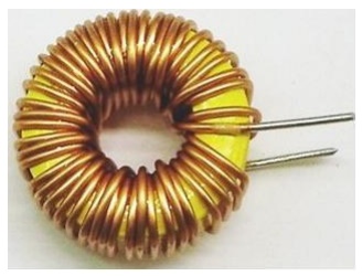
Inductors:
An inductor is an electronic device which consists of a coil of wire which may have a metallic or ferrite core. If it appears to have no core, it is considered to have an air core. The core material will greatly affect the value of the inductor. The unit of measure is the 'henry', but since that is such a large value of inductance, the value is usually stated in millihenries. One henry is equal to one thousand millihenries. If everything else stays constant, increasing the number of turns of wire around the core, will increase the value of the inductor.
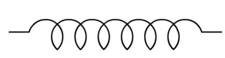
This is the schematic symbol for an inductor.
Inductor symbol:
An "ideal inductor" has inductance, but no resistance or capacitance, and does not dissipate energy. A real inductor is equivalent to a combination of inductance, some resistance due to the resistivity of the wire, and some capacitance. At some frequency, usually much higher than the working frequency, a real inductor behaves as a resonant circuit (due to its self capacitance). In addition to dissipating energy in the resistance of the wire, magnetic core inductors may dissipate energy in the core due to hysteresis, and at high currents may show other departures from ideal behavior due to nonlinearity.
Application of Inductor:
Inductors are used as surge protectors because they block strong current changes.
They are used as telephone line filters, to remove high frequency broadband signals and are placed on the ends of the cables to reduce signal noise.
Inductors and capacitors are used together in audio circuits to filter or amplify specific frequencies.
Chokes are small inductors that block alternating current and are used to reduce electrical and radio interference. A basic transformer is just two inductors wound around a large steel core. Their magnetic fields are coupled, because the core forces them to flow through both coils.
When an alternating current flows in one coil, it induces an alternating current in the other coil.
How Inductors Works:
The inductor has as a coil of copper conductors wound around a central core. When current is passed through the coil a magnetic flux is created around the coil due to the properties of electromotive force. The resistance increases when a core is placed in the coil and this increases the inductance by hundreds of times. The core can be made of different materials but cores made of ferrite produce the maximum inductance. The current to voltage lag is 90° but with the use of resistive substance a resistive and inductive circuit is formed, the phase angle lag becomes smaller and is based on the frequency that is constant.
Inductance is the circuit's resistance to change in current. Inductance tolerance is the amount of variation that is permitted within the nominal value. The frequency for which the distributed capacitance starts resonating with the inductance and canceling the capacitance is called the self resonant frequency or SRF. At SRF, the inductor works as a high impedance, resistive element. Quality factor (Q value) is the measure of relative losses of the inductor and is expressed as capacitive resistance divided by the equivalent serial resistance.
Inductors are used
1. In tuning circuits
2. In filter
3. In timing circuits
4. In oscillator tank circuits
Capacitors:
A capacitor or condenser is a passive electronic component consisting of a pair of conductors separated by a dielectric. When a voltage potential difference exists between the conductors, an electric field is present in the dielectric. This field stores energy and produces a mechanical force between the plates. The effect is greatest between wide, flat, parallel, narrowly separated conductors.
An ideal capacitor is characterized by a single constant value, capacitance, which is measured in farads. This is the ratio of the electric charge on each conductor to the potential difference between them. In practice, the dielectric between the plates passes a small amount of leakage current. The conductors and leads introduce an equivalent series resistance and the dielectric has an electric field strength limit resulting in a breakdown voltage.
The properties of capacitors in a circuit may determine the resonant frequency and quality factor of a resonant circuit, power dissipation and operating frequency in a digital logic circuit, energy capacity in a high-power system, and many other important aspects
Active components:
An electronic component is any physical entity in an electronic system whose intention is to affect the electrons or their associated fields in a desired manner consistent with the intended function of the electronic system. Components are generally intended to be in mutual electromechanical contact, usually by being soldered to a printed circuit board (PCB), to create an electronic circuit with a particular function (for example an amplifier, radio receiver, or oscillator). Components may be packaged singly or in more complex groups as integrated circuits. Some common electronic components are capacitors , resistors , diodes ,transistors, etc.
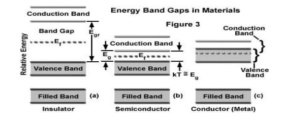
Semiconductor
A semiconductor is a solid material that has electrical conductivity between those of a conductor and an insulator.
A material with electrical conductivity due to electron flow intermediate in magnitude between that of a conductor and an insulator.
This means a conductivity roughly in the range of 103 to 10−8 siemens per centimeter.
Silicon is the most widely used semiconductor material.
The number of electrons in the valence orbit is the key to conductivity. ![]() Conductors have one valence electron, semiconductors have four valence electrons, and insulators have eight valence electrons.
Conductors have one valence electron, semiconductors have four valence electrons, and insulators have eight valence electrons.
Classification:
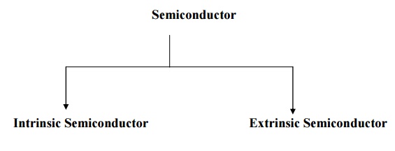
Semiconductor
1.Intrinsic Semiconductor
2.Extrinsic Semiconductor
Intrinsic Semiconductor:
![]() An intrinsic semiconductor also called an undoped semiconductor or i-type semiconductor.
An intrinsic semiconductor also called an undoped semiconductor or i-type semiconductor.
![]() It is a pure semiconductor without any significant dopant species present.
It is a pure semiconductor without any significant dopant species present.
![]() The number of charge carriers determined by the properties of the material itself instead of the amount of impurities.
The number of charge carriers determined by the properties of the material itself instead of the amount of impurities.
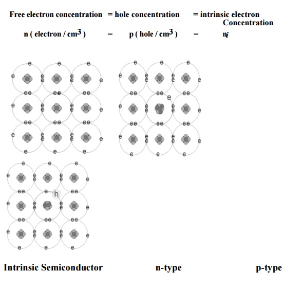
![]() In intrinsic semiconductors the number of excited electrons and the number of holes are equal: n = p.
In intrinsic semiconductors the number of excited electrons and the number of holes are equal: n = p.
Conductivity of Intrinsic semiconductor:
Ø The electrical conductivity of intrinsic semiconductors can be due to crystal defects or to thermal excitation.
Ø Both electrons and holes contribute to current flow in an intrinsic semiconductor.
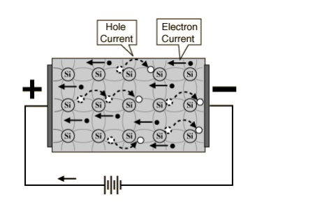
Ø The current which will flow in an intrinsic semiconductor consists of both electron and hole current.
Ø That is, the electrons which have been freed from their lattice positions into the conduction band can move through the material.
Ø In addition, other electrons can hop between lattice positions to fill the vacancies left by the freed electrons.
Ø This additional mechanism is called hole conduction because it is as if the holes are migrating across the material in the direction opposite to the free electron movement.
Ø The current flow in an intrinsic semiconductor is influenced by the density of energy states which in turn influences the electron density in the conduction band.
Ø This current is highly temperature dependent.
Thermal excitation:
Ø In an intrinsic semiconductor like silicon at temperatures above absolute zero, there will be some electrons which are excited across the band gap into the conduction band and which can produce current.
Ø When the electron in pure silicon crosses the gap, it leaves behind an electron vacancy or "hole" in the regular silicon lattice.
Ø Under the influence of an external voltage, both the electron and the hole can move across the material.
Ø In n-type semiconductor:
• The dopant contributes extra electrons, dramatically increasing the conductivity.
Ø In p-type semiconductor,
• The dopant produces extra vacancies or
holes, which likewise increase the conductivity.
Extrinsic Semiconductor
![]() The electrical conductivity of a pure semiconductor is very small.
The electrical conductivity of a pure semiconductor is very small.
![]() To increase the conductivity, impurities are added.
To increase the conductivity, impurities are added.
![]() The impurity added semiconductor is called extrinsic semiconductor.
The impurity added semiconductor is called extrinsic semiconductor.
![]() The process of adding impurity is called doping.
The process of adding impurity is called doping.
![]() The added impurity is called dopant.
The added impurity is called dopant.
![]() Usually one or two atoms of impurity is added per 106 atoms of a semiconductor.
Usually one or two atoms of impurity is added per 106 atoms of a semiconductor.
![]() There are two types (i) p-type and (ii) n-type semiconductors.
There are two types (i) p-type and (ii) n-type semiconductors.
(i) n-type semiconductor:
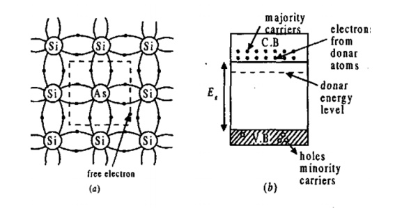
• When an impurity, from V group elements like arsenic (As), antimony having 5 valence electrons is added to Ge (or Si), the impurity atom donates one electron to Ge (or Si).
• The 4 electrons of the impurity atom is engaged in covalent bonding with Si atom.
• The fifth electron is free. This increases the conductivity.
• The impurities are called donors.
• The impurity added semiconductor is called n-type semiconductor, because their increased conductivity is due to the presence of the negatively charged electrons, which are called the majority carriers.
• The energy band of the electrons donated by the impurity atoms is just below the conduction band.
• The electrons absorb thermal energy and occupy the conduction band.
• Due to the breaking of covalent bond, there will be a few holes in the valence band at this temperature.
• These holes in n-type are called minority carriers.
(ii) p-type semiconductor:
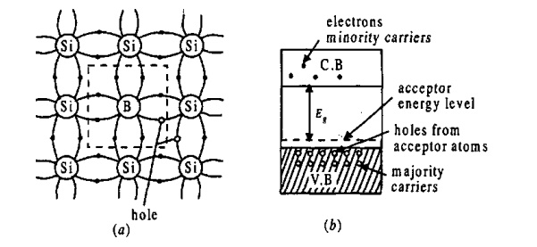
• If a III group element, like indium (In), boron (B), aluminium (AI) etc., having three valence electrons, is added to a semiconductor say Si, the three electrons form covalent bond.
• There is a deficiency of one electron to complete the 4th covalent bond and is called a hole.
• The presence of the hole increases the conductivity because these holes move to the nearby atom, at the same time the electrons move in the opposite direction.
• The impurities added semiconductor is called p-type semiconductor.
• The impurities are called acceptors as they accept electrons from the semiconductor
• Holes are the majority carriers and the electrons produced by the breaking of bonds are the minority carriers.
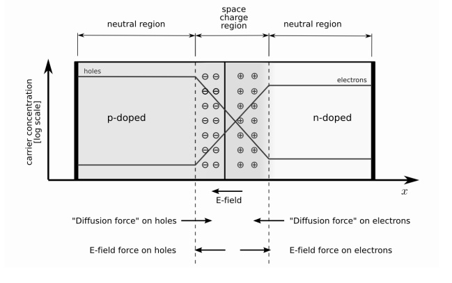
PN Junction Diode
A p–n junction is formed by joining P-type and N-type semiconductors together in very close contact.
The term junction refers to the boundary interface where the two regions of the semiconductor meet.
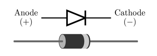
Diode is a two-terminal electronic component that conducts electric current in only one direction.
The crystal conducts conventional current in a direction from the p-type side (called the anode) to the n-type side (called the cathode), but not in the opposite direction.
Biasing:
There are two operating regions and three possible "biasing" conditions for the standard Junction Diode and these are:
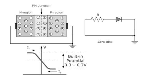
Zero Bias - No external voltage potential is applied to the PN-junction. -When a diode is Zero Biased no external energy source is applied and a natural Potential Barrier is developed across a depletion layer.
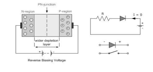
Reverse Bias - The voltage potential is connected negative, (-ve) to the P- type material and positive, (+ve) to the N-type material across the diode which has the effect of Increasing the PN-junction width.
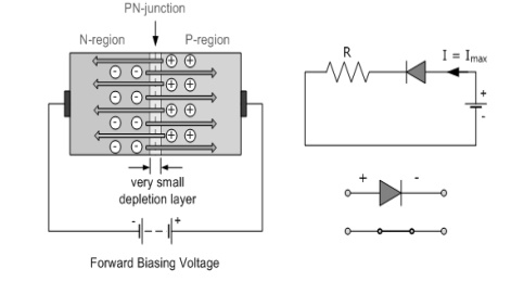
-When a junction diode is Forward Biased the thickness of the depletion region reduces and the diode acts like a short circuit allowing full current to flow.
Forward Bias - The voltage potential is connected positive, (+ve) to the P-t ype material and negative, (-ve) to the N-type material across the diode which has the effect of Decreasing the PN- junction width.
- When a junction diode is Reverse Biased the thickness of the depletion region increases and the diode acts like an open circuit blocking any current flow, (only a very small leakage current).
V-I Characteristics:
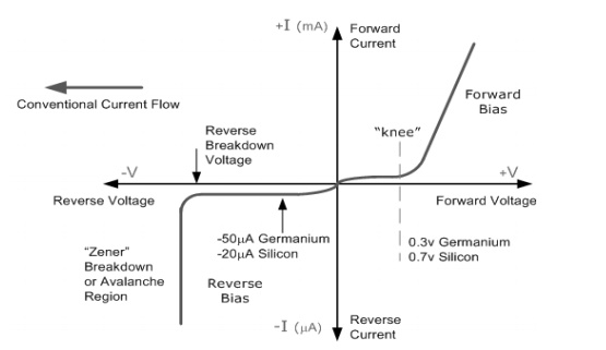
Forward Bias:
The application of a forward biasing voltage on the junction diode results in the depletion layer becoming very thin and narrow which represents a low impedance path through the junction thereby allowing high currents to flow.
The point at which this sudden increase in current takes place is represented on the static I-V characteristics curve above as the "knee" point.
Reverse Bias:
In Reverse biasing voltage a high resistance value to the PN junction and practically zero current flows through the junction diode with an increase in bias voltage.
However, a very small leakage current does flow through the junction which can be measured in microamperes, (μA).
One final point, if the reverse bias voltage Vr applied to the diode is increased to a sufficiently high enough value, it will cause the PN junction to overheat and fail due to the avalanche effect around the junction.
This may cause the diode to become shorted and will result in the flow of maximum circuit current, and this shown as a step downward slope in the reverse static characteristics curve below.
Energy Band Structure:
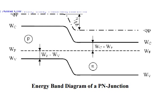
Energy Band Diagram of a PN-Junction
Diffusion capacitance and Space Charge capacitance
Diffusion capacitance
v As a p-n diode is forward biased, the minority carrier distribution in the quasi-neutral region increases dramatically.
v In addition, to preserve quasi-neutrality, the majority carrier density increases by the same amount.
v This effect leads to an additional capacitance called the diffusion capacitance.
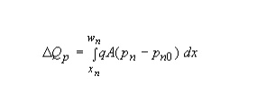
v The diffusion capacitance is calculated from the change in charge with voltage:
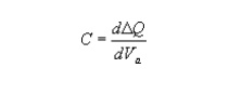
Where the charge, DQ, is due to the excess carriers.
Unlike a parallel plate capacitor, the positive and negative charge is not spatially separated. Instead, the electrons and holes are separated by the energy bandgap.
Nevertheless, these voltage dependent charges yield a capacitance just as the one associated with a parallel plate capacitor.
The excess minority-carrier charge is obtained by integrating the charge density over the quasi-neutral region:
Space Charge capacitance:
v After joining p-type and n-type semiconductors, electrons near the p–n interface tend to diffuse into the p region.
v As electrons diffuse, they leave positively charged ions (donors) in the n region.
v Similarly, holes near the p–n interface begin to diffuse into the n-type region leaving fixed ions (acceptors) with negative charge.
v The regions nearby the p–n interfaces lose their neutrality and become charged, forming the space charge capacitance.
Zener Diode
A Zener diode is a special kind of diode which permits current to flow in the forward direction as normal, but will also allow it to flow in the reverse direction when the voltage is above a certain value-the breakdown voltage known as the Zener voltage.
V-I Characteristics of the Zenor Diode:
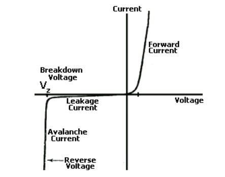
• The illustration above shows this phenomenon in a current vs voltage graph with a zener diode connected in the forward direction .It behaves exactly as a standard diode.
• In the reverse direction however there is a very small leakage current between 0v and the zener voltage –i.e. just a tiny amount of current is able to flow.
• Then, when the voltage reaches the breakdown voltage(vz),suddenly current can flow freely through it.
Zenor Diode voltage regulator circuit
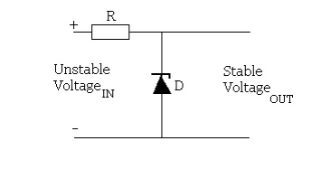
• Since the voltage dropped across a Zener diode is a known and fixed value,Zener diode are typically used to regulate the voltage in electric circuits.
• Using a resistor to ensure that the current passing through the Zener diode is atleast 5mA.
• The voltage drop across the diode is exactly equal to the Zener voltage of the diode.
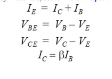
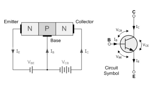
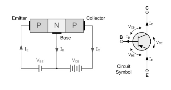
BJT
A bipolar junction transistor (BJT) is a three-terminal electronic device constructed of doped semiconductor material.
It may be used in amplifying or switching applications.
Bipolar transistors are so named because their operation involves both electrons and holes.
Charge flow in a BJT is due to bidirectional diffusion of charge carriers across a junction between two regions of different charge concentrations.
3 adjacent regions of doped Si (each connected to a lead):
o Base. (thin layer,less doped).
o Collector.
o Emitter.
2 types of BJT:
o npn.
o pnp.
npn bipolar junction transistor:
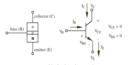
npn bipolar junction transistor
• 1 thin layer of p-type, sandwiched between 2 layers of n-type.
• N-type of emitter: more heavily doped than collector.
• With VC>VB>VE:
– Base-Emitter junction forward biased, Base-Collector reverse biased.
– Electrons diffuse from Emitter to Base (from n to p).
– There‘s a depletion layer on the Base-Collector junction -- -- > no flow of e- allowed.
– BUT the Base is thin and Emitter region is n+ (heavily doped) -- -- > electrons have enough momentum to cross the Base into the Collector.
– The small base current IB controls a large current IC
pnp bipolar junction transistor:
pnp bipolar junction transistor
• 1 thin layer of n-type, sandwiched between 2 layers of p-type.
• P-type of emitter: more heavily doped than collector.
• The voltages vEB and vCB are positive when they forward bias their respective pn junctions.
• Collector current and base current exit the transistor terminals and emitter current enters the device.
• Base current is given by:
Emitter current is given by:
Operation of NPN and NPN Transistor
Operation of NPN Transistor:
Forward-biased junction:
With the emitter-to-base junction in the figure biased in the forward direction, electrons leave the negative terminal of the battery and enter the n- material (emitter).
Since electrons are majority current carriers in the n- material, they pass easily through the emitter, cross over the junction, and combine with holes in the p material (base).
For each electron that fills a hole in the p material, another electron will leave the p material (creating a new hole) and enter the positive terminal of the battery.
Reverse-biased junction:
The second pn- junction (base-to-collector), or reverse-biased junction as it is called blocks the majority current carriers from crossing the junction.
However, there is a very small current, that does pass through this junction.
This current is called minority current, or reverse current. This current was produced by the electron-hole pairs.
The minority carriers for the reverse-biased pn- junction are the electrons in the p material and the holes in the n- material.
These minority carriers actually conduct the current for the reverse-biased junction when electrons from the p material enter the n material, and the holes from the n- material enter the p- material.
However, the minority current electrons play the most important part in the operation of the npn transistor.
Total current flow in the npn transistor is through the emitter lead. Therefore, in terms of percentage, IE is 100 percent.
On the other hand, since the base is very thin and lightly doped, a smaller percentage of the total current (emitter current) will flow in the base circuit than in the collector circuit.
Usually no more than 2 to 5 percent of the total current is base current (IB) while the remaining 95 to 98 percent is collector current (IC).
A very basic relationship exists between these two currents:
IE = IB + IC
Operation of PNP Transistor:
Forward Biased Junction:
With the bias setup shown, the positive terminal of the battery repels the emitter holes toward the base, while the negative terminal drives the base electrons toward the emitter.
When an emitter hole and a base electron meet, they combine.
For each electron that combines with a hole, another electron leaves the negative terminal of the battery, and enters the base.
At the same time, an electron leaves the emitter, creating a new hole, and enters the positive terminal of the battery.
This movement of electrons into the base and out of the emitter constitutes base current flow (IB), and the path these electrons take is referred to as the emitter-base circuit.
Reverse Biased Junction:
In the reverse-biased junction the negative voltage on the collector and the positive voltage on the base block the majority current carriers from crossing the junction.
However, this same negative collector voltage acts as forward bias for the minority current holes in the base, which cross the junction and enter the collector.
The minority current electrons in the collector also sense forward bias-the positive base voltage-and move into the base.
The holes in the collector are filled by electrons that flow from the negative terminal of the battery.
At the same time the electrons leave the negative terminal of the battery, other electrons in the base break their covalent bonds and enter the positive terminal of the battery.
Although there is only minority current flow in the reverse-biased junction, it is still very small because of the limited number of minority current carriers.
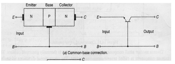
Transistor Configuration
CE, CB, CC Configurations:
We know that transistor has three terminals namely emitter(E), base(B), collector(C).
However, when a transistor is connected in a circuit, we require four terminals (ie) two terminals for input and two terminals for output. This difficulty is overcome by using one of the terminals as common terminal.
Depending upon the terminals which are used as a common terminal to the input and output terminals, the transistors can be connected in the following three different configuration.
1. Common base configuration
2. Common emitter configuration
3. Common collector configuration
Common base configuration:
In this configuration base terminal is conncted as a common terminal. The input is applied between the emitter and base terminals.The output is taken between the collector and base terminals.
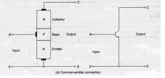
Common emitter configuration:
In this configuration emitter terminal is conncted as a common terminal.
The input is applied between the base and emitter terminals.The output is taken between the collector and base terminals.
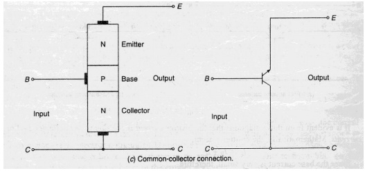
Common collector configuration:
In this configuration collector terminal is conncted as a common terminal.
The input is applied between the base and collector terminals.The output is taken between the emitter and collector terminals
CB, CE,CC Characteristics :
1. Common base Characteristics :
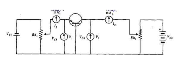
Input characteristics:
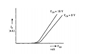
v The output(CB) voltage is maintained constant and the input voltage (EB) is set at several convenient levels. For each level of input voltage, the input current IE is recorded.
v IE is then plotted versus VEB to give the common-base input characteristics.
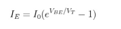
v The EB junction is essentially the same as a forward biased diode, therefore the current-voltage characteristics is essentially the same as that of a diode:
Output characteristics:
The emitter current IE is held constant at each of several fixed levels. For each fixed value of IE , the output voltage VCB is adjusted in convenient steps and the corresponding levels of collector current IC are recorded.
.For each fixed value of IE, IC is almost equal to IE and appears to remain constant when VCB is increased.
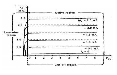
2.Common-Emitter Characteristics :
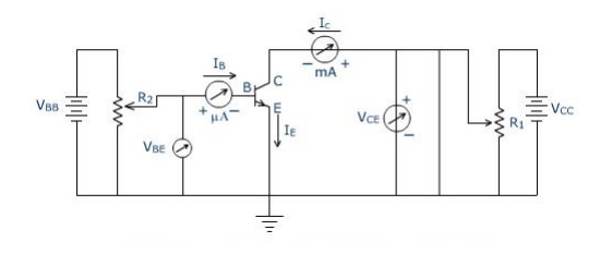
Input characteristics:
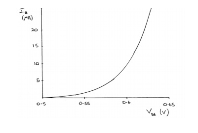
v The output voltage VCE is maintained constant and the input voltage VBE is set at several convenient levels.For each level of input voltage, the input current IB is recorded.
v IB is then plotted versus VBE to give the common-base input characteristics.
Output characteristics:
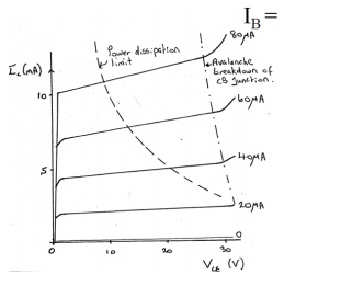
The Base current IB is held constant at each of several fixed levels. For each fixed value of IB , the output voltage VCE is adjusted in convenient steps and the corresponding levels of
collector current IC are recorded
v .For each fixed value of IB, IC level is Recorded at each VCE step.For each IB level, IC is plotted versus VCE to give a family of characteristics.
3.Common-Collector Characteristics :
![]()
Input characteristics:
v The common-collector input characteristics are quite different from either common base or common-emitter input characteristics.
v The difference is due to the fact that the input voltage (VBC)
is largely determined by (VEC) level .
VEC = VEB + VBC
VEB = VEC - VBC
Output characteristics:
The operation is much similar to that of C-E configuration.When the base current is ICO, the emitter current will be zero and consequently no current will flow in the load.
When the base current is increased, the transistor passes through active region and eventually reaches saturation.
Under the saturation conditions all the supply voltage, except for a very small drop across the transistor will appear across the load resistor.
Early Effect and Early Voltage
Base-Width Modulation:
v As reverse-bias across the collector-base junction increases, the width of the collector-base depletion layer increases and the effective width of base decreases.
v This is called ―base-width modulation‖.
Early effect:
When the output characteristics are extrapolated back to where the iC curves intersect at common point, vCE = -VA (Early voltage), which lies between 15 V and 150 V.
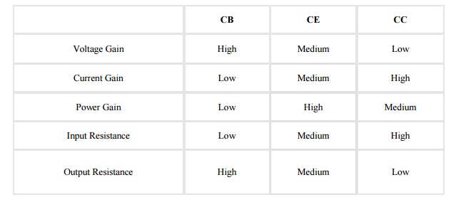
Comparison of the CB, CE, and CC Configurations
Related Topics