Chapter: RF and Microwave Engineering : RF Transistor Amplifier Design and Matching Networks
RF Transistor Amplifier Design and Matching Networks
RF TRANSISTOR AMPLIFIER DESIGN AND MATCHING NETWORKS
1. AMPLIFIER POWER RELATION
2. STABILITY CONSIDERATION AND FREQUENCY RESPONSE:
ü Unconditional stability: The network is unconditionally stable if[ Гin] <1 and [Гout]<1 for all passive source and load impedances(i.e Гs<1 and ГL<1)
ü Conditional stability: The network is conditionally stable if |_in| < 1 and |_out| < 1 only for a
certain range of passive source and load impedances. This case is also referred to as potentially unstable.
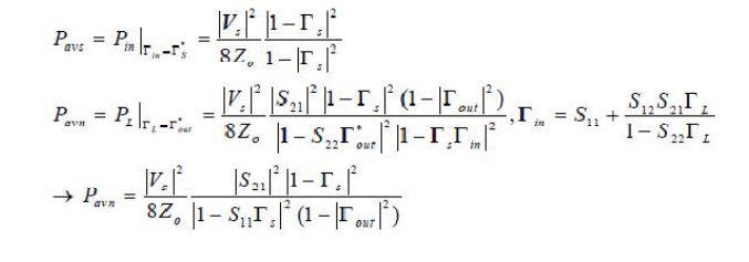
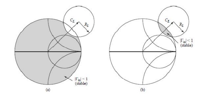
Stability Circles
ü Applying the above requirements for unconditional stability to (12.3) gives the following conditions that must be satisfied by _S and _L if the amplifier is to be unconditionally
ü We can derive the equation for the output stability circle as follows. First use (12.19a) to express the condition that |_in| = 1 as
3. GAIN CONSIDERATION NOISE FIGURE
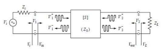
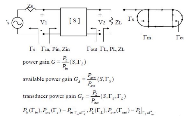
Consider an arbitrary two-port network, characterized by its scattering matrix [S], connected to source and load impedances ZS and ZL , respectively, as shown in Figure 12.1.
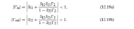
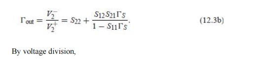
We will derive expressions for three types of power gain in terms of the scattering parameters of the two-port network and the reflection coefficients, _S and _L , of the source and load. Power gain = G = PL/Pin is the ratio of power dissipated in the load ZL to the power delivered to the input of the two-port network.
This gain is independent of ZS, although the characteristics of some active devices may be dependent on ZS.
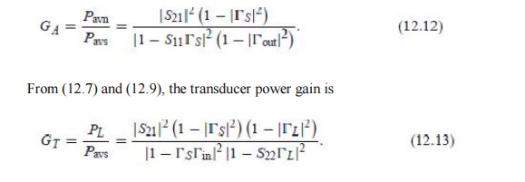
Available power gain = GA = Pavn/Pavs is the ratio of the power available from the two-port network to the power available from the source.
This assumes conjugate matching of both the source and the load, and depends on ZS, but not ZL . _
Transducer power gain = GT = PL/Pavs is the ratio of the power delivered to the load to the power available from the source. This depends on both ZS and ZL .
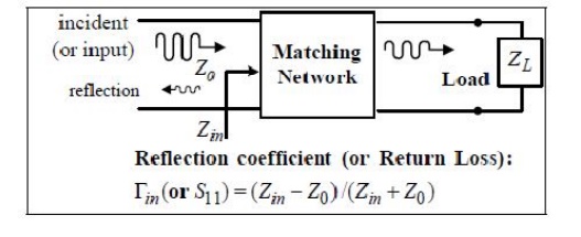
These definitions differ primarily in the way the source and load are matched to the twoport device; if the input and output are both conjugately matched to the two-port device, then the gain is maximized and G = GA = GT . With reference to Figure 12.1, the reflection coefficient seen looking toward the load is
while the reflection coefficient seen looking toward the source is
where Z0 is the characteristic impedance reference for the scattering parameters of the two-port network. the following analysis. From the definition of the scattering parameters, and the fact that V+ 2 = _LV− 2 , we have
where Zin is the impedance seen looking into port 1 of the terminated network. Similarly, the reflection coefficient seen looking into port 2 of the network when port 1 is terminated by ZS is
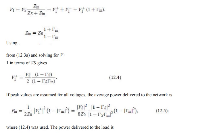
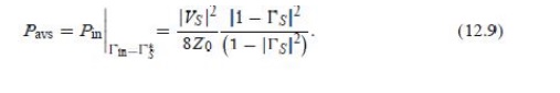
The power available from the source, Pavs, is the maximum power that can be delivered to the network. This occurs when the input impedance of the terminated network is conjugately matched to the source impedance, as discussed in Section 2.6. Thus, from (12.5),
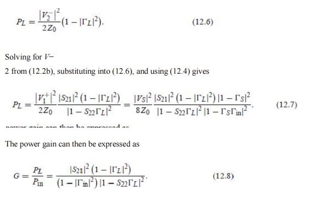
Similarly, the power available from the network, Pavn, is the maximum power that can be delivered to the load. Thus, from (12.7),
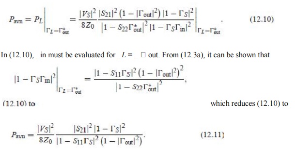
Observe that Pavs and Pavn have been expressed in terms of the source voltage, VS, which is independent of the input or load impedances. There would be confusion if these quantities were expressed in terms of V+ 1 since V+ 1 is different for each of the calculations of PL , Pavs, and Pavn. Using (12.11) and (12.9), we obtain the available power gain as
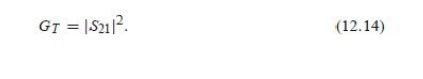
A special case of the transducer power gain occurs when both the input and output are matched for zero reflection (in contrast to conjugate matching). Then _L = _S = 0, and (12.13) reduces to
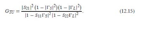
Another special case is the unilateral transducer power gain, GTU, where S12 = 0 (or is negligibly small). This nonreciprocal characteristic is approximately true for many transistors devices. From (12.3a),
_in = S11 when S12 = 0, so (12.13) gives the unilateral transducer power gain as
4. IMPEDANCE MATCHING NETWORKS
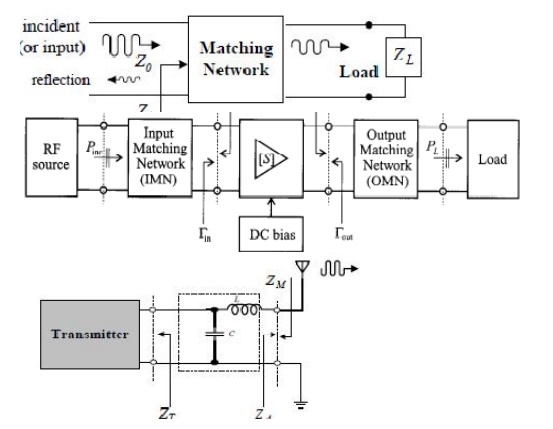
Impedance matching (or tuning) is important for the following reasons
ü minimum power loss in the feed line & maximum power delivery
ü linearizing the frequency response of the circuit
ü improving the S/N ratio of the system for sensitive receiver components (lownoise amplifier, etc.)
ü reducing amplitude & phase errors in a power distribution network (such as antenna array-feed network)
Factors in the selection of matching networks
ü complexity -bandwidth requirement (such as broadband design) - adjustability
ü implementation (by using transmission line, chip R/L/C elements ..)
5. T AND PI MATCHNIG NETWORKS
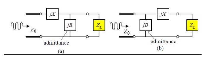
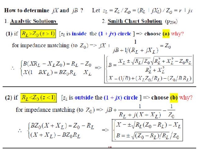
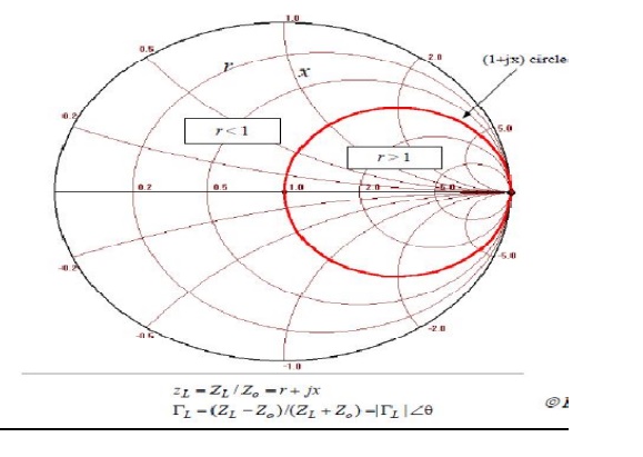
L-section Networks (Two-component )
Lumped elements: R/L/C
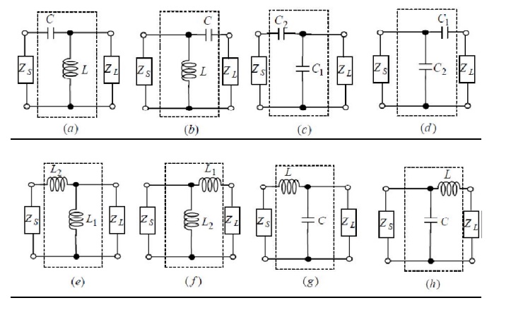
T- section Networks
π- section Networks
Matching with Lumped Elements: L-section Network
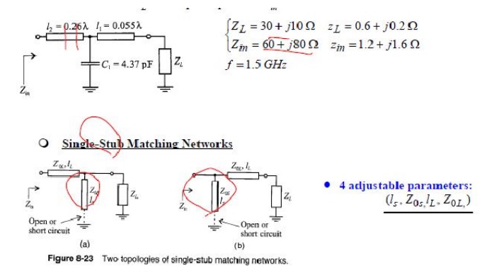
6. MICROSTRIP MATCHING NETWORKS
Microstrip Line Matching Networks
ü In the mid-GHz and higher frequency range, the discrete R/L/C lumped elements will have more noticeable parasitic effects (see chapter 2) and let to complicating the circuit design process
ü Distributed components such as transmission line segments can be used to mix with lumped elements
From Discrete Components to Microstrip Lines
ü Avoid using inductors (if possible) due to higher resistive loss (& higher price)
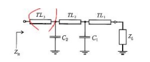
ü In general, one shunt capacitor & two series transmission lines is sufficiently to transform any load to any input impedance.
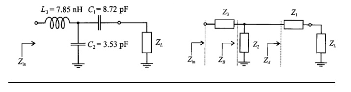
EX: transform load ZL to an input impedance Zin
Related Topics