Chapter: Embedded Systems Design : Interfacing to the analogue world
Power control in Interfacing to the analogue
Power control
Most embedded designs need to be able to switch power in some way or
another, if only to drive an LED or similar indicator. This, on first
appearances, appears to be quite simple to do but there are some traps that can
catch designers out. This section goes through the basic principles and
techniques.
Matching the drive
The first problem that faces any design is matching the logic level
voltages with that of a power transistor or similar device. It is often
forgotten or assumed that with logic devices, a logical high is always 5 volts
and that a logical low is zero. A logical high of 5 volts is more than enough
to saturate a bipolar transistor and turn it on. Similarly, 0 volts is enough
to turn off such a transistor.
Unfortunately, the specifications for TTL compatible logic levels are
not the same as indicated by these assumptions. The voltage levels are define a
logic low output as any voltage below a maximum which is usually 0.4 volts and
a logic high output as a voltage above 2.4 volts assuming certain bus
capacitance and load currents and a supply voltage of 4.5 to 5.5 volts. These
figures are typical and can vary.
If the output high is used to drive a bipolar transistor, then the 2.4
volt value is high enough to turn on the transistor. The only concern is the
current drive that the output can provide. This value times the gain of the
transistor determines the current load that the transistor can provide. With an
output low voltage of 0.4 volts, the situation is less clear and is dependent
on the biasing used on the transistor. It is possible that instead of turning
the transistor off completely, it partially turns the device off and some
current is still provided.
With CMOS logic levels, similar problems can occur. Here the logic high
is typically two thirds of the supply voltage or higher and a logic low is one
third of the supply voltage or lower. With a 5 volt supply, this works out at
3.35 volts and 1.65 volts for the high and low states. In this case, the low
voltage is above the 0.7 volts needed to turn on a transistor and thus the
transistor is likely to be switched on all the time irrespective of the logic
state. These voltage mismatches can also cause problems when combin-ing CMOS
and TTL devices using a single supply. With bipolar transistors there are
several techniques that can be used to help avoid these problems:
•
Use a high gain transistor
The higher the gain of the transistor, the lower the drive needed from
the output pin and the harder the logic level will be. If the required current
is high, then the voltage on the output is more likely to reach its limits.
With an output high, it will fall to the minimum value. With an output low, it
will rise to the maximum value.
Darlington transistor pairs are often used because they have a far
higher gain compared to a single transistor.
•
Use a buffer pack
Buffer packs are logic devices that have a high drive capa-bility and
can provide higher drive currents than normal logic outputs. This increased
drive capability can be used to drive an indicator directly or can be further
amplified.
•
Use a field effect transistor
(FET)
These transistors are voltage controlled and have a very high effective
gain and thus can be used to switch heavy loads easily from a logic device.
There are some problems, however, in that the gate voltages are often
proportions of the supply voltages and these do not match with the logic
voltage levels that are available. As a result, the FET does not switch
correctly. This problem has been solved by the introduction of logic level
switching FETs that will switch using standard logic voltages. The advantage
that these offer is that they can simply have their gate directly con-nected to
the logic output. The power supply and load are connected through the FET which
acts as a switch.
Using H bridges
Using logic level FETs is a very simple and effective way of providing
DC power control. With the FET acting like a power switch whose state reflects
the logic level output from the digital controller, it is possible to combine
several switches to create H bridges which allow a DC motor to be switched on
and reversed in direction. This is done by using two outputs and four FETs
acting as switches.
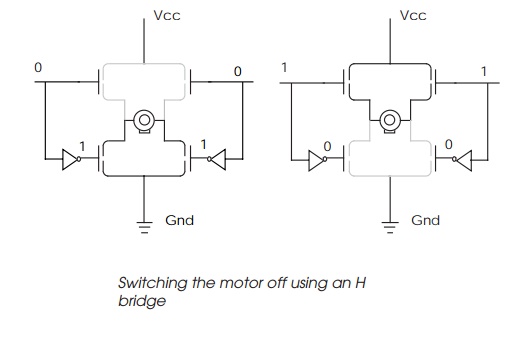
The FETs are arranged in two pairs so that by switching one on and the
other off, one end of the motor can be connected to ground (0 volts) or to the
voltage supply Vcc. Each FET in the pair is driven from a common input signal
which is inverted on its way to one of the FETs. This ensures that only one of
the pairs switches on in response to the input signal. With the two pairs, two
input signals are needed. When these signals are the same, i.e. 00 or 11,
either the top or bottom pairs of FETS are switched on and no voltage
differential is applied across the motor, so nothing hap-pens. This is shown in
the first diagram where the switched-on paths are shown in black and the
switched-off paths are in grey.
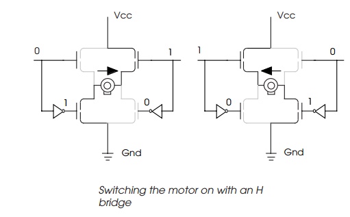
If the input signals are different then a top and a bottom FET is
switched on and the voltage is applied across the motor and it revolves. With a
01 signal it moves in one direction and with a 10 signal it moves in the
reverse direction.
This type of bridge arrangement is frequently used for controlling DC
motors or any load where the voltage may need reversing.
Driving LEDs
Light emitting diodes (LEDs) are often used as indicators in digital
systems and in many cases can simply be directly driven from a logic output
provided there is sufficient current and voltage drive.
The voltage drive is necessary to get the LED to illuminate in the first
place. LEDs will only light up when their diode reverse breakdown voltage is
exceeded. This is usually about 2 to 2.2 volts and less than the logic high
voltage. The current drive determines how bright the LED will appear and it is
usual to have a current limiting resistor in series with the LED to prevent it
from drawing too much current and overheating. For a logic device with a 5 volt
supply a 300 Ω resistor will limit the current to about 10 mA. The problem comes if
the logic output is only 2.4 or 2.5 volts and not the expected 5 volts. This
means that the resistor is sufficient to drop enough voltage so that the LED
does not light up. The solution is to use a buffer so that there is sufficient
current drive or alterna-tively use a transistor to switch on the LED. There
are special LED driver circuits packs available that are designed to connect
di-rectly to an LED without the need for the current limiting resistor. The
resistor or current limiting circuit is included inside the device.
Interfacing to relays
Another method of switching power is to use a mechanical relay where the
logic signal is used to energise the relay. The relay contacts make or break
accordingly and switch the current. The advantage of a relay is that it can be
used to switch either AC or DC power and there is no electrical connections
between the low power relay coil connected to the digital circuits and the
power load that is being switched. As a result, they are frequently used to
switch high loads.
Relays do suffer from a couple of problems. The first is that the relay
can generate a back voltage across its terminals when the energising current is
switched off, i.e. when the logic output switches from a high to a low. This
back EMF as it is known can be a high voltage and cause damage to the logic
circuits. A logic output does not expect to see an input voltage differential
of several tens of volts! The solution is to put a diode across the relay
circuits so that in normal operation, the diode is reverse biased and does
nothing. When the back EMF is generated, the diode starts to conduct and the
voltage is shorted out and does no damage. This problem is experienced with any
coil, including those in DC motors. It is advisable to fit a diode when driving
these compo-nents as well.
The other problem is that the switch contacts can get sticky where they
are damaged with the repeated current switching. This can erode the contacts
and cause bad contacts or in some cases can cause local overheating so that the
contacts weld themselves together. The relay is now sticky in that the contacts
will not change when the coil is de-energised.
Interfacing to DC motors
So far with controlling DC motors, the emphasis has been simple on-off
type switching. It is possible with a digital system to actually provide speed
control using a technique called pulse width modulation.
With a DC motor, there are two techniques for controlling the motor
speed: the first is to reduce the DC voltage to the motor. The higher the
voltage, the faster it will turn. At low voltages, the control can be a bit hit
and miss and the power control is ineffi-cient. The alternative technique
called pulse width modulation (PWM) will control a motor speed not by reducing
the voltage to the motor but by reducing the time that the motor is switched
on.
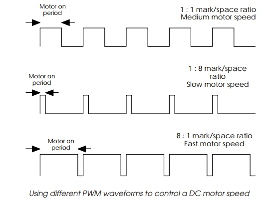
This is done by generating a square wave at a frequency of several
hundred hertz and changing the mark/space ratio of the wave form. With a large
mark and a low space, the voltage is applied to the motor for almost all of the
cycle time, and thus the motor will rotate very quickly. With a small mark and
a large space, the opposite is true. The diagram shows the waveforms for
medium, slow and fast motor control.
The only difference between this method of control and that for a simple
on-off switch is the timing of the pulses from the digital output to switch the
motor on and off. There are several methods that can be used to generate these
waveforms.
Software only
With a software-only system, the waveform timing is done by creating
some loops that provide the timing functions. The program pseudo code shows a
simple structure for this. The first action is to switch the motor on and then
to start counting through a delay loop. The length of time to count through the
delay loop determines the motor-on period. When the count is finished, the
motor is switched off. The next stage is to count through a second delay loop
to determine the motor-off period.
repeat
(forever)
{
switch
on motor delay loop1 switch off motor delay loop2
}
This whole procedure is repeated for as long as the motor needs to be
driven. By changing the value of the two delays, the mark/space ratio of the
waveform can be altered. The total time taken to execute the repeat loop gives
the frequency of the wave-form. This method is processor intensive in that the
program has to run while the motor is running. On first evaluation, it may seem
that while the motor is running, nothing else can be done. This is not the
case. Instead of simply using delay loops, other work can be inserted in here
whose duration now becomes part of the timing for the PWM waveform. If the work
is short, then the fine control over the mark/space ratio is not lost because
the contribution that the work delay makes compared to the delay loop is small.
If the work is long, then the minimum motor-on time and thus motor speed is
determined by this period.
repeat
(forever)
{
switch
on motor perform task a delay loop1 switch off motor delay loop2
}
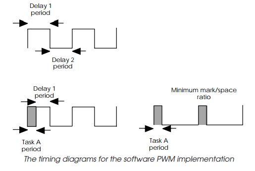
The timing diagrams for the software loop PWM wave-forms are shown in
the diagrams above. In general, software only timing loops are not efficient
methods of generating PWM wave-forms for motor control. The addition of a
single timer greatly improves the mechanism.
Using a single timer
By using a single timer, PWM waveforms can be created far easier and
free up the processor to do other things without impacting the timing. There
are several methods that can be used to do this. The key principle is that the
timer can be programmed to create a periodic interrupt.
Method 1 — using the timer to
define the on period
With this method, the timer is used to generate the on period. The
processor switches the motor on and then starts the timer to count down. While
the timer is doing this, the processor is free to do what ever work is needed.
The timer will eventually time out and generate a processor interrupt. The processor
serv-ices the interrupt and switches the motor off. It then goes into a delay
loop still within the service routine until the time period arrives to switch
the motor on again. The processor switches the motor on, resets the timer and
starts it counting and continues with its work by returning from the interrupt
service routine.
Method 2 — using the timer to
define frequency period
With this method, the timer is used to generate a periodic interrupt
whose frequency is set by the timer period. When the processor services the
interrupt, it uses a software loop to deter-mine the on period. The processor
switches on the motor and uses the software delay to calculate the on period.
When the delay loop is completed, it switches off the motor and can continue
with other work until the timer generates the next interrupt.
Method 3 — using the timer to
define both the on and off periods
With this method, the timer is used to generate both the on and off
periods. The processor switches the motor on, loads the timer with the
on-period value and then starts the timer to count down. While the timer is
doing this, the processor is free to do what ever work is needed. The timer
will eventually time out and generate a processor interrupt, as before. The
processor services the interrupt and switches the motor off. It then loads the
timer with the value for the off period. The processor then starts the timer
counting and continues with its work by returning from the interrupt service
routine.
The timer now times out and generates an interrupt. The processor
services this by switching the motor on, loading the timer with the one delay
value and setting the timer counting before returning from the interrupt.
As a result, the processor is only involved when interrupted by the
timer to switch the motor on or off and load the timer with the appropriate
delay value and start it counting. Of all these three methods, this last method
is the most processor efficient. With methods 1 and 2, the processor is only
free to do other work when the mark/space ratio is such that there is time to
do it. With a long motor-off period, the processor performs the timing in
software and there is little time to do anything else. With a short motor-off
period, there is more processing time and far more work can be done. The
problem is that the work load that can be achieved is dependent on the
mark/space ratio of the PWM waveform and engine speed. This can be a major
restriction and this is why the third method is most commonly used.
Using multiple timers
With two timers, it is possible to generate PWM waveforms with virtually
no software intervention. One timer is setup to generate a periodic output at
the frequency of the required PWM waveform. This output is used to trigger a
second timer which is configured as a monostable. The second timer output is
used to provide the motor-on period. If these timers are set to automati-cally
reload, the first timer will continually trigger the second and thus generate a
PWM waveform. By changing the delay value in the second timer, the PWM
mark/space ratio can be altered as needed.
Related Topics