Chapter: Electronic Devices : Power Devices and Display Devices
Photo transistors - Photo junction Devices
PHOTO JUNCTION DEVICES
Photo
junction Devices are basically PN-Junction light sensors or detectors made from
silicon semiconductor PN-junctions which are sensitive to light and which can
detect both visible light and infra-red light levels. Photo-junction devices
are specifically made for sensing light and this class of photoelectric light
sensors include the Photodiode and the Phototransistor.
PHOTO TRANSISTORS
An
alternative photo-junction device to the photodiode is the Phototransistor
which is basically a photodiode with amplification. The Phototransistor light
sensor has its collector-base PN-junction reverse biased exposing it to the
radiant light source.
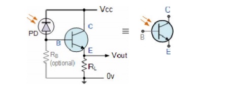
Figure 5.38 Photo-transistor Symbol
Photo transistors
operate the same as the photodiode except that they can provide current gain
and are much more sensitive than the photodiode with currents are 50 to 100
times greater than that of the standard photodiode and any normal transistor
can be easily converted into a phototransistor light sensor by connecting a
photodiode between the collector and base.
Phototransistors
consist mainly of a bipolar NPN Transistor with its large base region
electrically unconnected, although some phototransistors allow a base
connection to control the sensitivity, and which uses photons of light to
generate a base current which in turn causes a collector to emitter current to
flow. Most phototransistors are NPN types whose outer casing is either
transparent or has a clear lens to focus the light onto the base junction for
increased sensitivity.
Photo-transistor Construction and Characteristics
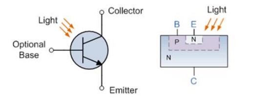
Figure 5.39 phototransistor
construction
In the
NPN transistor the collector is biased positively with respect to the emitter
so that the base/collector junction is reverse biased. therefore, with no light
on the junction normal leakage or dark current flows which is very small. When
light falls on the base more electron/hole pairs are formed in this region and
the current produced by this action is amplified by the transistor.
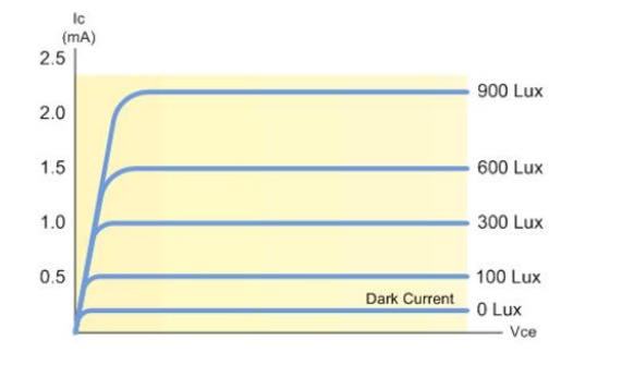
Figure 5.40 V-I characteristics
of phototransistor
Usually
the sensitivity of a phototransistor is a function of the DC current gain of
the transistor. Therefore, the overall sensitivity is a function of collector
current and can be controlled by connecting a resistance between the base and
the emitter but for very high sensitivity optocoupler type applications,
Darlington phototransistors are generally used.
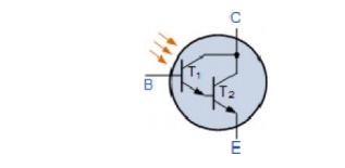
Figure 5.41 Darlington
phototransistors symbol
Applications
Phototransistors are used for a wide variety of
applications. In fact, phototransistors can be used in any electronic device
that senses light. For example, phototransistors are often used in smoke
detectors, infrared receivers, and CD players. Phototransistors can also be
used in astronomy, night vision, and laser range-finding.
Some of the areas of application for the
phototransistor include punch-card readers, computer logic circuitry, lighting
control (highways, etc.), level indication, relays, and counting systems.
Advantages
Phototransistors
have several important advantages that separate them from other optical
sensors. They produce a higher current than photodiodes and also produce a
voltage, something that photoresistors cannot do. Phototransistors are very
fast and their output is practically instantaneous. They are relatively
inexpensive, simple, and so small that several of them can fit onto a single
integrated computer chip.
Disadvantages
While
phototransistors can be advantageous, they also have several disadvantages.
Phototransistors made of silicon cannot handle voltages over 1,000 Volts. They
do not allow electrons to move as freely as other devices, such as electron
tubes, do. Also, phototransistors are also more vulnerable to electrical
surges/spikes and electromagnetic energy.
Related Topics