Chapter: Basic Electrical and Electronics Engineering
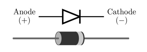
PN Junction Diode
PN Junction Diode
A p–n junction is formed by joining P-type and N-type semiconductors together in very close contact.
The term junction refers to the boundary interface where the two regions of the semiconductor meet.
Diode is a two-terminal electronic component that conducts electric current in only one direction.
The crystal conducts conventional current in a direction from the p-type side (called the anode) to the n-type side (called the cathode), but not in the opposite direction.
Biasing:
There are two operating regions and three possible "biasing" conditions for the standard Junction Diode and these are:
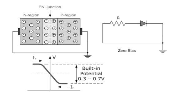
Zero Bias - No external voltage potential is applied to the PN-junction. -When a diode is Zero Biased no external energy source is applied and a natural Potential Barrier is developed across a depletion layer.
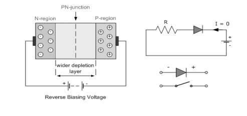
Reverse Bias - The voltage potential is connected negative, (-ve) to the P- type material and positive, (+ve) to the N-type material across the diode which has the effect of Increasing the PN-junction width.
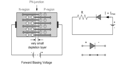
-When a junction diode is Forward Biased the thickness of the depletion region reduces and the diode acts like a short circuit allowing full current to flow.
Forward Bias - The voltage potential is connected positive, (+ve) to the P-t ype material and negative, (-ve) to the N-type material across the diode which has the effect of Decreasing the PN- junction width.
- When a junction diode is Reverse Biased the thickness of the depletion region increases and the diode acts like an open circuit blocking any current flow, (only a very small leakage current).
V-I Characteristics:
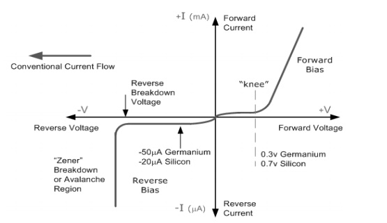
Forward Bias:
The application of a forward biasing voltage on the junction diode results in the depletion layer becoming very thin and narrow which represents a low impedance path through the junction thereby allowing high currents to flow.
The point at which this sudden increase in current takes place is represented on the static I-V characteristics curve above as the "knee" point.
Reverse Bias:
In Reverse biasing voltage a high resistance value to the PN junction and practically zero current flows through the junction diode with an increase in bias voltage.
However, a very small leakage current does flow through the junction which can be measured in microamperes, (μA).
One final point, if the reverse bias voltage Vr applied to the diode is increased to a sufficiently high enough value, it will cause the PN junction to overheat and fail due to the avalanche effect around the junction.
This may cause the diode to become shorted and will result in the flow of maximum circuit current, and this shown as a step downward slope in the reverse static characteristics curve below.
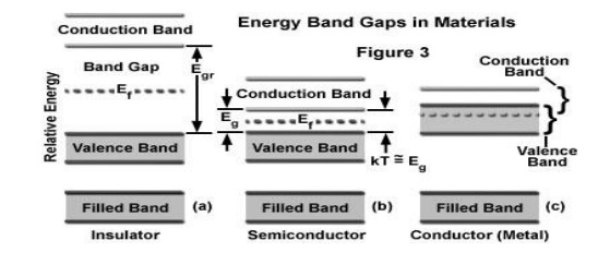
Energy Band Structure:
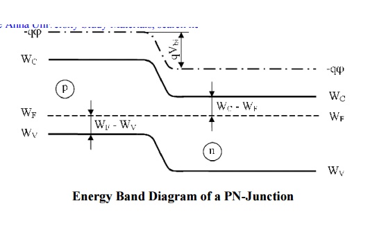
Energy Band Diagram of a PN-Junction
Diffusion capacitance and Space Charge capacitance
Diffusion capacitance
v As a p-n diode is forward biased, the minority carrier distribution in the quasi-neutral region increases dramatically.
v In addition, to preserve quasi-neutrality, the majority carrier density increases by the same amount.
v This effect leads to an additional capacitance called the diffusion capacitance.
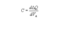
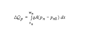
v The diffusion capacitance is calculated from the change in charge with voltage:
Where the charge, DQ, is due to the excess carriers.
Unlike a parallel plate capacitor, the positive and negative charge is not spatially separated. Instead, the electrons and holes are separated by the energy bandgap.
Nevertheless, these voltage dependent charges yield a capacitance just as the one associated with a parallel plate capacitor.
The excess minority-carrier charge is obtained by integrating the charge density over the quasi-neutral region:
Space Charge capacitance:
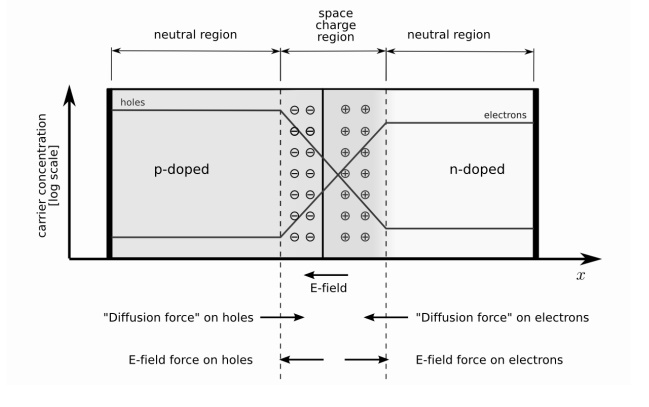
v After joining p-type and n-type semiconductors, electrons near the p–n interface tend to diffuse into the p region.
v As electrons diffuse, they leave positively charged ions (donors) in the n region.
v Similarly, holes near the p–n interface begin to diffuse into the n-type region leaving fixed ions (acceptors) with negative charge.
v The regions nearby the p–n interfaces lose their neutrality and become charged, forming the space charge capacitance.
Related Topics