Chapter: Digital Principles and System Design : Boolean Algebra and Logic Gates
NAND and NOR implementation
NAND and NOR implementation
Any logic function can be implemented using NAND gates. To
achieve this, first the logic function has to be written in Sum of Product
(SOP) form. Once logic function is converted to SOP, then is very easy to
implement using NAND gate. In other words any logic circuit with AND gates in
first level and OR gates in second level can be converted into a NAND-NAND gate
circuit.
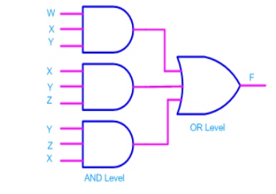
Consider
the following SOP expression
F = W.X.Y
+ X.Y.Z + Y.Z.W
The above expression can be implemented with three AND gates
in first stage and one OR gate in second stage as shown in figure.
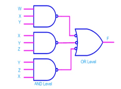
If bubbles are introduced at AND
gates output and OR gates inputs (the same for NOR gates), the above circuit
becomes as shown in figure.
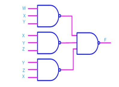
Now replace OR gate with input
bubble with the NAND gate. Now we have circuit which is fully implemented with
just NAND gates.
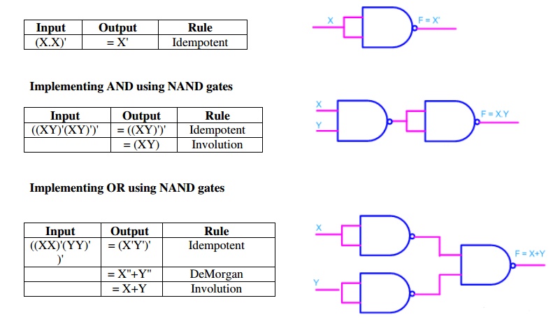
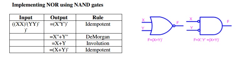
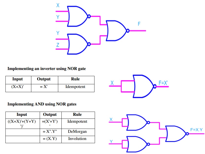
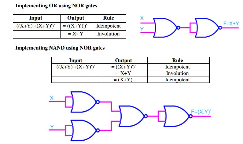
ü Realization of logic gates using NAND gates
Implementing
an inverter using NAND gate
ü
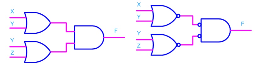
Realization of logic function using NOR gates
Any logic function can be implemented using NOR gates. To
achieve this, first the logic function has to be written in Product of Sum
(POS) form. Once it is converted to POS, then it's very easy to implement using
NOR gate. In other words any logic circuit with OR gates in first level and AND
gates in second level can be converted into a NOR-NOR gate circuit.
Consider
the following POS expression
F = (X+Y)
. (Y+Z)
The above expression can be implemented with three OR gates in
first stage and one AND gate in second stage as shown in figure.
If bubble are introduced at the output of the OR gates and the
inputs of AND gate, the above circuit becomes as shown in figure.
Now replace AND gate with input bubble with the NOR gate. Now
we have circuit which is fully implemented with just NOR gates.
Minimization
Technique
The primary objective of all simplification procedures is to
obtain an expression that has the minimum number of terms. Obtaining an
expression with the minimum number of literals is usually the secondary
objective. If there is more than one possible solution with the same number of
terms, the one having the minimum number of literals is the choice.
There are several methods for simplification of Boolean logic
expressions. The process is usually called logic minimization and the goal is
to form a result which is efficient. Two methods we will discuss are algebraic
minimization and Karnaugh maps. For very complicated problems the former method
can be done using special software analysis programs. Karnaugh maps are also
limited to problems with up to 4 binary inputs. The Quine–McCluskey
tabular method is used for more than 4 binary inputs.
Ref: 1) A.P Godse & D.A Godse “Digital Electronics”, Technical publications, Pune, Revised edition, 2008. Pg.No:3.78
2) Morris Mano M. and Michael D. Ciletti, “Digital Design”, IV Edition, Pearson Edition 2008.Pg.No:89.
Related Topics