Chapter: Embedded Systems Design : Embedded processors
Motorola MC68020
Motorola MC68020
The MC68020 was launched in April 1984 as the ‘32 bit performance
standard’ and in those days its performance was simply staggering — 8 million
instructions per second peak with 2–3 million sustained when running at 16 MHz
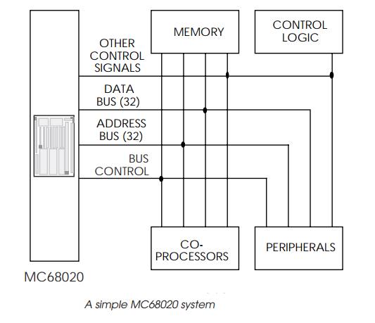
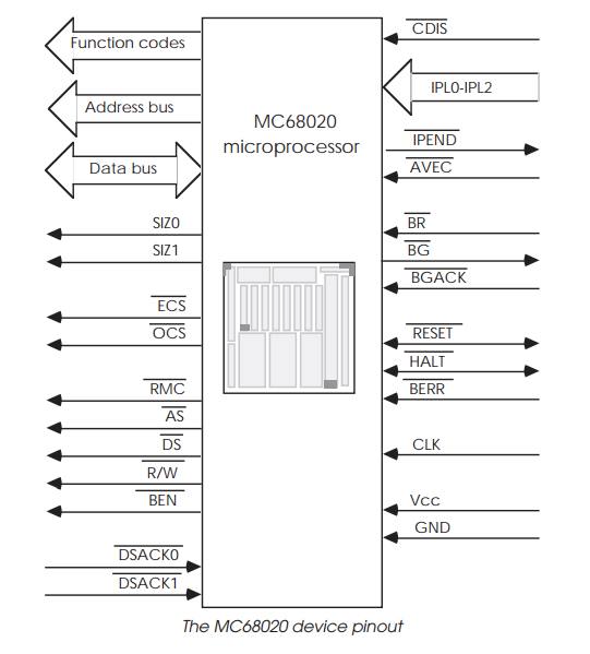
clock speed. It was a true 32 bit processor with 32 bit wide external data and
address buses as shown. It supported all the features and functions of the
MC68000 and MC68010, and it executed M68000 USER binary code without
modification (but faster!).
•
Virtual memory and instruction
continuation were sup-ported. This is explained in Chapter 7 on interrupts.
•
The bus and control signals were
similar to that of its M68000 predecessors, offering an asynchronous memory
interface but with a three–cycle operation (instead of four) and dynamic bus
sizing which allowed the processor to talk to 8, 16 and 32 bit processors.
•
Additional coprocessors could be
added to provide such facilities as floating point arithmetic and memory
manage-ment, which used this bus to provide a sophisticated com-munications
interface.
•
The instruction set was enhanced
with more data types, addressing modes and instructions.
•
Bit field data and its
manipulation was supported, along with packed and unpacked BCD (binary coded
decimal) formats. An instruction cache and a barrel shifter to per-form high
speed shift operations were incorporated on-chip to provide support for these
functions.
The actual pipeline used within the design is quite sophis-ticated. It
is a four–stage pipe with stage A consisting of an instruction router which
accepts data from either the external bus controller or the internal cache. As
the instruction is processed down the pipeline, the intermediate data can
either cause micro and nanocode sequences to be generated to control the
execution unit or, in the case of simpler instructions, the data itself can be
passed directly into the execution unit with the subsequent speed improvements.
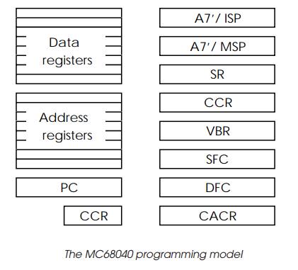
The programmer’s model
The programmer’s USER model is exactly the same as for the MC68000,
MC68010 and MC68008. It has the same eight data and eight address 32 bit
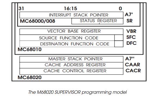
register organisation. The SUPERVISOR mode is a superset of its predecessors.
It has all the registers found in its predecessors plus another three. Two
registers are associated with controlling the instruction cache, while the
third provides the master stack pointer.
The supervisor uses either its master stack pointer or inter-rupt stack
pointer, depending on the exception cause and the status of the M bit in the
status register. If this bit is clear, all stack operations default to the A7´
stack pointer. If it is set, interrupt stack frames are stored using the
interrupt stack pointer while other operations use the master pointer. This
effectively allows the system to maintain two separate stacks. While primarily
for operating system support, this extra register can be used for high
reliability designs.
The MC68020 instruction set is a superset of the MC68000/ MC68010 sets.
The main difference is the inclusion of floating point and coprocessor
instructions, together with a set to manipu-late bit field data. The
instructions to perform a trap on condition operation, a compare and swap
operation and a ‘call-return from module’ structure were also included. Other
differences were the addition of 32 bit displacements for the LINK and Bcc
(branch on condition) instructions, full 32 bit arithmetic with 32 or 64 bit
results as appropriate and extended bounds checking for the CHK (check) and CMP
(compare) instructions.
The bit field instructions were included to provide addi-tional support
for applications where data does not conveniently fall into a byte
organisation. Telecommunications and graphics both manipulate data in odd sizes
— serial data can often be 5, 6 or 7 bits in size and graphics pixels (i.e.
each individual dot that makes a picture on a display) vary in size, depending
on how many colours, grey scales or attributes are being depicted.
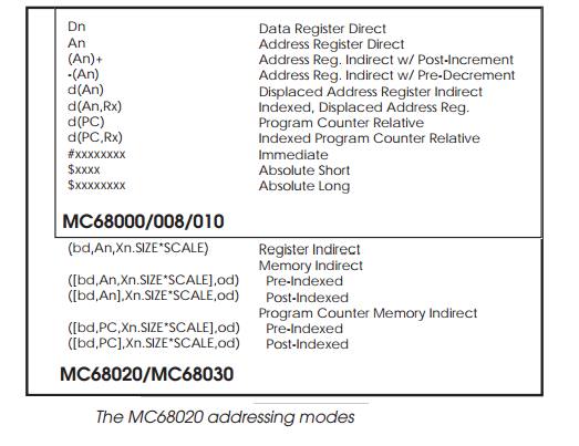
The addressing modes were extended from the basic M68000 modes, with
memory indirection and scaling. Memory indirec-tion allowed the contents of a
memory location to be used within an effective address calculation rather than
its absolute address. The scaling was a simple multiplier value 1, 2, 4 or 8 in
magnitude, which multiplied (scaled) an index register. This allowed large data
elements within data structures to be easily accessed without having to perform
the scaling calculations prior to the access. These new modes were so complex
that even the differentiation between data and address registers was greatly
reduced: with the MC68020, it is possible to use data registers as additional
address registers. In practice, there are over 50 variations available to the
programmer to apply to the 16 registers.
The new CAS and CAS2 ‘compare and swap’ instructions provided an elegant
solution to linked list updating within a multiprocessor system. A linked list
is a series of data lists linked together by storing the address of the next
list in the chain in the preceding chain. To add or delete a list simply
involves modifying these addresses.
In a multiprocessor system, this modification procedure must occur
uninterrupted to prevent corruption. The CAS and CAS2 instruction meets this
specification. The current pointer to the next list is read and stored in Dn.
The new value is calculated and stored in Dm. The CAS instruction is then
executed. The current pointer value is read and compared with Dn. If they are
the same, no other updating by another processor has happened and Dm is written
out to update the list. If they do not match, the value is copied into Dn,
ready for a repeat run. This sequence is per-formed using an indivisible
read-modify-write cycle. The condi-tion codes are updated during each stage.
The CAS2 instruction performs a similar function but with two sets of values.
This instruction is also performed as a series of indivisible cycles but with
different addresses appearing during the execution.
Bus interfaces
Many of the signals shown in the pin out diagram are the same as those
of the MC68000 — the function codes FC0–2, interrupt pins IPL0–2 and the bus
request pins, RESET*, HALT* and BERR* perform the same functions.
With the disappearance of the M6800 style interface, sepa-rate signals
are used to indicate an auto-vectored interrupt. The AVEC* signal is used for
this function and can be permanently asserted if only auto-vectored interrupts
are required. The IPEND signal indicates when an interrupt has been internally
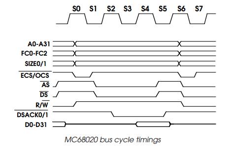
recognised and awaits an acknowledgement cycle. RMC* indicates an indi-visible
read-modify-write cycle instead of simply leaving AS* asserted between the bus
cycles. The address strobe is always released at the end of a cycle. ECS* and
OCS* provide an early warning of an impending bus cycle, and indicate when
valid address information is present on the bus prior to validation by the
address strobe.
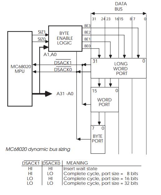
The M68000 upper and lower data strobes have been re-placed by A0 and
the two size pins, SIZE0 and SIZE1. These indicate the amount of data left to
transfer on the current bus cycle and, when used with address bits A0 and A1,
can provide decode information so that the correct bytes within the 4 byte wide
data bus can be enabled. The old DTACK* signal has been replaced by two new
ones, DSACK0* and DSACK1*. They provide the old DTACK* function of indicating a
successful bus cycle and are used in the dynamic bus sizing. The bus interface
is asynchronous and similar to the M68000 cycle but with a shorter three–cycle
se-quence, as shown.
Related Topics