Phase Locked Loop (PLL) - Monolithic PLL IC 565 applications | Linear Integrated Circuits : Analog Multiplier and PLL
Chapter: Linear Integrated Circuits : Analog Multiplier and PLL
Monolithic PLL IC 565 applications
Monolithic
PLL IC 565 applications:
The
output from a PLL system can be obtained either as the voltage signal vc(t)
corresponding to the error voltage in the feedback loop, or as a frequency
signal at VCO output terminal. The voltage output is used in frequency
discriminator applications whereas the frequency output is used in signal conditioning,
frequency synthesis or clock recovery applications.
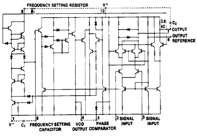
The circuit diagram of LM565 PLL
When
PLL is locked to an input frequency, the error voltage vc(t) is proportional to
(fs-fo). If the input frequency is varied as in the case of FM signal vc will
also vary in order to maintain the lock. Thus the voltage output serves as a
frequency discriminator which converts the input frequency changes to voltage
changes.
In
the case of frequency output, if the input signal is comprised of many
frequency components corrupted with noise and other disturbances, the PLL can
be made to lock, selectively on one particular frequency component at the
input. The output of VCO would then regenerate that particular frequency
(because of LPF which gives output for beat frequency) and attenuate heavily
other frequencies. VCO output thus can be used for regenerating or
reconditioning a desired frequency signal (which is weak and buried in noise)
out of many undesirable frequency signals.
Some
of the typical applications of PLL are discussed below.
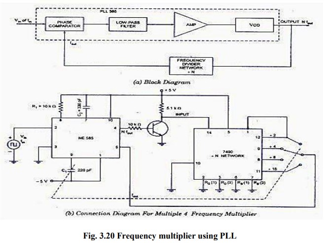
Frequency Multiplier:
Frequency
divider is inserted between the VCO & phase comparator. Since the output of
the divider is locked to the fIN, VCO is actually running at a multiple of the
input frequency.
The
desired amount of multiplication can be obtained by selecting a proper
divide-by-N network, where N is an integer.
Frequency Shift Keying (FSK) demodulator:
In
computer peripheral & radio (wireless) communication the binary data or code
is transmitted by means of a carrier frequency that is shifted between two
preset frequencies. Since a carrier frequency is shifted between two preset
frequencies, the data transmission is said to use a FSK. The frequency
corresponding to logic 1 & logic 0 states are commonly called the mark
& space frequency.
For
example, When transmitting teletype writer information using a
modulator-demodulator (modem) a 1070-1270 (mark-space) pair represents the
originate signal, while a 2025-2225 Hz (mark-space) pair represents the answer
signal.
FSK Generator:
·
The
FSK generator is formed by using a 555 as an astable multivibrator, whose
frequency is controlled by the state of transistor Q1.
·
In
other words, the output frequency of the FSK generator depends on the logic
state of the digital data input.
·
150
Hz is one the standards frequencies at which the data are commonly transmitted.
·
When
the input is logic 1, the transistor Q1 is off. Under the condition, 555 timer
works in its normal mode as an astable multivibrator i.e., capacitor C charges
through RA & RB to 2/3 Vcc &
discharges through RB to 1/3 Vcc. Thus capacitor C charges & discharges
between 2/3 Vcc & 1/3 Vcc as long as the input is logic 1.
·
The
frequency of the output waveform is given
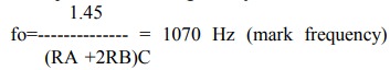
·
When
the input is logic 0, (Q1 is ON saturated) which in turn connects the
resistance Rc across RA. This action reduces the charging time of
capacitor C1 increases the output frequency, which is given by,
·
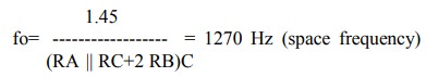
By
proper selection of resistance Rc, this frequency is adjusted to equal the
space frequency of 1270 Hz. The difference between the FSK signals of 1070 Hz
& 1270 Hz is 200 Hz, this difference is called “frequency shift”.
·
The
output 150 Hz can be made by connecting a voltage comparator between the output
of the ladder filter and pin 6 of PLL.
·
The
VCO frequency is adjusted with R1 so that at fIN = 1070
Hz.
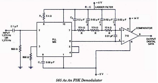
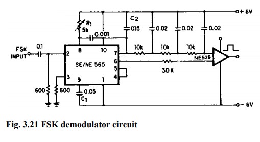
FSK Demodulator:
·
The
output of 555 FSK generators is applied to the 565 FSK demodulator.
·
Capacitive
coupling is used at the input to remove dc line.
·
At
the input of 565, the loop locks to the input frequency & tracks it between
the 2 frequencies.
·
R1
& C1 determine the free running frequency of the VCO, 3 stages RC ladder
filter is used to remove the carrier component from the output.
Applications:
In
digital data communication and computer peripheral, binary data is transmitted
by means of a carrier frequency which is shifted between two preset
frequencies. This type of data transmission is called frequency shift keying
(FSK) technique. The binary data can be retrieved using FSK demodulator. The
figure below shows FSK demodulator using PLL for tele-typewriter signals of
1070 Hz and 1270 Hz. As the signal appears at the input, the loop locks to the
input frequency and tracks it between the two frequencies with a corresponding
dc shift at the output. A three stage filter removes the carrier component and
the output signal is made logic compatible by a voltage comparator.
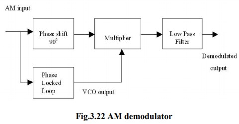
AM Demodulation:
A
PLL may be used to demodulate AM signals as shown in the figure below. The PLL
is locked to the carrier frequency of the incoming AM signal. The output of VCO
which has the same frequency as the carrier, but unmodulated is fed to the
multiplier. Since VCO output is always 900 before being fed to the
multiplier. This makes both the signals applied to the multiplier and the
difference signals, the demodulated output is obtained after filtering high
frequency components by the LPF. Since the PLL responds only to the carrier frequencies
which are very close to the VCO output, a PLL AM detector exhibits high degree
of selectivity and noise immunity which is not possible with conventional peak
detector type AM modulators.
FM Demodulation:
If
PLL is locked to a FM signal, the VCO tracks the instantaneous frequency of the
input signal. The filtered error voltage which controls the VCO and maintains
lock with the input signal is the demodulated FM output.
The
VCO transfer characteristics determine the linearity of the demodulated output.
Since, VCO used in IC PLL is highly linear, it is possible to realize highly
linear FM demodulators.
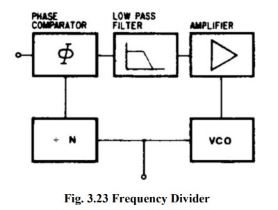
Frequency multiplication/division:
The
block diagram shown below shows a frequency multiplier/divider using PLL. A
divide by N network is inserter between the VCO output and the phase comparator
input. In the locked state, the VCO output frequency fo is given by fo
= Nfs. The multiplication factor can be obtained by selecting a
proper scaling factor N of the counter.
Frequency
multiplication can also be obtained by using PLL in its harmonic locking mode.
If the input signal is rich in harmonics e.g. square wave, pulse train etc.,
then the VCO can be directly locked to the n-th harmonic of the input signal
without connecting any frequency divider in between. However, as the amplitude
of the higher order harmonics becomes less, effective locking may not take
place for high values of n. Typically n is kept less than 10.
The
circuit of the figure above can also be used for frequency division. Since the
VCO
output
(a square wave) is rich in harmonics, it is possible to lock the m-th harmonic
of the VCO output with the input signal fs. The output fo of VCO is now given
by fo=fs/m
PLL Frequency Synthesis:
In
digital wireless communication systems (GSM, CDMA etc), PLL's are used to
provide the Local Oscillator (LO) for up-conversion during transmission, and
down-conversion during reception. In most cellular handsets this function has
been largely integrated into a single integrated circuit to reduce the cost and
size of the handset.
However
due to the high performance required of base station terminals, the
transmission and reception circuits are built with discrete components to
achieve the levels of performance required. GSM LO modules are typically built
with a Frequency Synthesizer integrated circuit, and discrete resonator VCO's.
Principle of PLL synthesizers
A
phase locked loop does for frequency what the Automatic Gain Control does for
voltage. It compares the frequencies of two signals and produces an error
signal which is proportional to the difference between the input frequencies.
The
error signal is then low pass filtered and used to drive a voltage-controlled
oscillator (VCO) which creates an output frequency. The output frequency is fed
through a frequency divider back to the input of the system, producing a
negative feedback loop.
If
the output frequency drifts, the error signal will increase, driving the
frequency in the opposite direction so as to reduce the error. Thus the output
is locked to the frequency at the
other input. This input is called the reference and is derived from a crystal
oscillator, which is very stable in frequency.
The
block diagram below shows the basic elements and arrangement of a PLL based
frequency synthesizer.
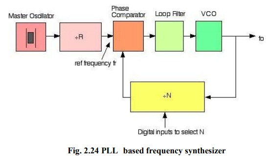
The
key to the ability of a frequency synthesizer to generate multiple frequencies
is the divider placed between the output and the feedback input. This is
usually in the form of a digital counter, with the output signal acting as a
clock signal.
The
counter is preset to some initial count value, and counts down at each cycle of
the clock signal. When it reaches zero, the counter output changes state and
the count value is reloaded.
This
circuit is straightforward to implement using flip-flops, and because it is
digital in nature, is very easy to interface to other digital components or a
microprocessor. This allows the frequency output by the synthesizer to be
easily controlled by a digital system.
Example:
Suppose
the reference signal is 100 kHz, and the divider can be preset to any value
between 1 and 100. The error signal produced by the comparator will only be
zero when the output of the divider is also 100 kHz. For this to be the case,
the VCO must run at a frequency which is 100 kHz x the divider count value.
Thus
it will produce an output of 100 kHz for a count of 1, 200 kHz for a count of
2, 1 MHz for a count of 10 and so on. Note that only whole multiples of the
reference frequency can be obtained with the simplest integer N dividers.
Fractional N dividers are readily available
Practical considerations:
In
practice this type of frequency synthesizer cannot operate over a very wide
range of frequencies, because the comparator will have a limited bandwidth and
may suffer from aliasing problems. This would lead to false locking situations,
or an inability to lock at all. In addition, it is hard to make a high
frequency VCO that operates over a very wide range.
This
is due to several factors, but the primary restriction is the limited
capacitance range of varactor diodes. However, in most systems where a
synthesizer is used, we are not after a huge range, but rather a finite number
over some defined range, such as a number of radio channels in a specific band.
Many
radio applications require frequencies that are higher than can be directly
input to the digital counter. To overcome this, the entire counter could be
constructed using high-speed logic such as ECL, or more commonly, using a fast
initial division stage called a prescaler
which reduces the frequency to a manageable level.
Since
the prescaler is part of the overall division ratio, a fixed prescaler can
cause problems designing a system with narrow channel spacing’s - typically
encountered in radio applications. This can be overcome using a dual-modulus
prescaler.
Further
practical aspects concern the amount of time the system can switch from channel
to channel, time to lock when first switched on, and how much noise there is in
the output. All of these are a function of the loop filter of the system, which is a low-pass filter placed
between the output of the frequency comparator and the input of the VCO.
Usually
the output of a frequency comparator is in the form of short error pulses, but
the input of the VCO must be a smooth noise- free DC voltage. (Any noise on
this signal naturally causes frequency modulation of the VCO.).
Heavy
filtering will make the VCO slow to respond to changes, causing drift and slow
response time, but light filtering will produce noise and other problems with
harmonics. Thus the design of the filter is critical to the performance of the
system and in fact the main area that a designer will concentrate on when
building a synthesizer system.
Related Topics