Chapter: High Voltage Engineering : Generation of High Voltages and High Currents
Impulse voltage generator circuits
Impulse voltage generator circuits
The
introduction to the full impulse voltages as defined in the previous section
leads to simple circuits for the generation of the necessary wave shapes. The
rapid increase and slow decay can obviously be generated by discharging
circuits with two energy storages, as the wave shape may well be composed by
the superposition of two exponential functions.
Again the
load of the generators will be primarily capacitive, as insulation systems are
tested. This load will therefore contribute to the stored energy. A second
source of energy could be provided by an inductance or additional capacitor.
For lightning impulses mainly, a fast discharge of pure inductor is usually
impossible, as h.v. chokes with high energy content can never be built without
appreciable stray capacitances. Thus a suitable fast discharge circuit will
always consist essentially of two capacitors.
Single-stage
generator circuits Two basic circuits for single-stage impulse generators are
shown in Fig. 3.21.The capacitor C1 is slowly charged from a dace.
source until the spark gap Gbreaks down. This spark gap acts as a
voltage-limiting and voltage-sensitive switch, whose ignition time (time to
voltage breakdown) is very short in comparison to T1. As such
single-stage generators may be used for charging voltages from some kV up to
about 1 MV, the sphere gaps) will offer proper operating conditions.
An
economic limit of the charging voltage V0 is, however, a value of about 200 to
250 kV, as too large diameters of the spheres would otherwise be required to
avoid excessive in homogeneous field distributions between the spheres. The
resistors R1, R2 and the capacitance C2 form
the wave shaping network. R1 will primarily damp the circuit and control the
front time T1. R2 will discharge the capacitors and
therefore essentially control the wave tail.
The
capacitance C2 represents the full load, i.e. the object under test
as well as all other capacitive elements which are in parallel to the test
object (measuring devices; additional load capacitor to avoid large variations
of T1/T2, if the test objects are changed). No
inductances are assumed so far, and are neglected in the first fundamental
analysis, which is also necessary to understand multistage generators. In
general this approximation is permissible, as the inductance of all circuit
elements has to be kept as low as possible.
Within
the ‘discharge’ capacitance C1. As C1 is always much larger than C2,
this figure determines mainly the cost of a generator. For the analysis we may
use the Laplace transform circuit sketched .which simulates the boundary
condition, that for t 0 C1 is charged to V0 and for t > 0 this capacitor is
directly connected to the wave shaping network. For the circuit Fig. 3.21(a)
the output voltage is thus given by the expression.
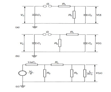
Figure:
3.21Single-stage impulse generator circuits (a) and (b). C1: discharge
capacitance. C2 : load capacitance. R1 : front or damping resistance. R2 :
discharge resistance. (c) Transform circuit Before starting the analysis, we
should mention the most significant parameter of impulse generators. This is
the maximum stored energy
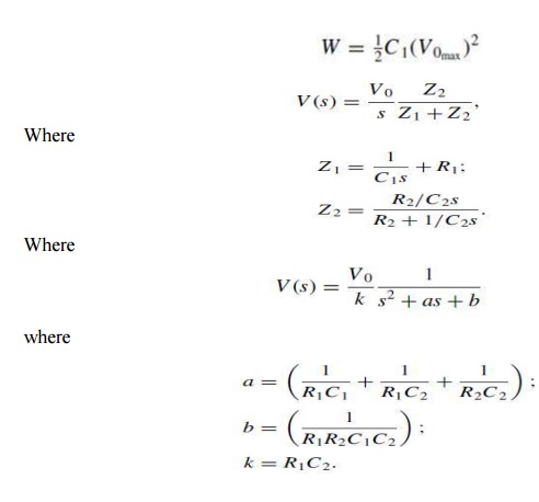
For
circuit Fig. 3.22 (b) one finds the same general expression eqn , with the
following constants; however,
For both
circuits, therefore, we obtain from the transform tables the same expression in
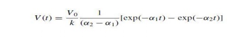
the time domain:
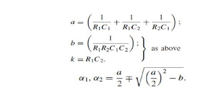
Although
one might assume that both circuits are equivalent, a larger difference may
occur if the voltage efficiency, 5, is calculated. This efficiency is defined
as
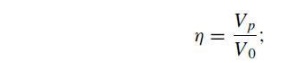
Vp being
the peak value of the output voltage as indicated . Obviously this value is
always smaller than 1 or 100 per cent. It can be calculated by finding tmax
from dVt/dt D0; this time for the voltage Vt to rise to its peak
value is given by
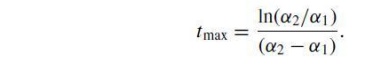
Substituting
this equation into eqn one may find
All these
equations contain the time constants 1/˛1 and 1/˛2, which depend upon the wave shape. There is,
however, no simple relationship between these time constants and the times T1,
T2 and Tp as defined in the national or international
recommendations, i.e. in Figs 2.23 and 2.24. This relationship can be found by
applying the definitions to the analytical expression for Vt,this means to
equation. The relationship is irrational and must be computed numerically. The
following table shows the result for some selected wave shapes: The
standardized nominal values of T1 and T2 are difficult to
achieve in practice, as even for fixed values of C1 the load C2
will vary and the exact values for R1 and R2 according to
above equation in general not available.
These
resistors have to be dimensioned for the rated high voltage of the generator
and are accordingly expensive. The permissible tolerances forT1 and
T2 are therefore necessary and used to graduate the resistor values.
According of the real output voltage V(t) will in addition be necessary if the
admissible impulse shape has to be testified. Another reason for such a
measurement is related to the value of the test voltage as defined in the
recommendations. This magnitude corresponds to the crest value, if the shape of
the lightning impulse is smooth.
However,
oscillations or an overshoot may occur at the crest of the impulse. If the
frequency of such oscillations is not less than 0.5MHz or the duration of
overshoot not over 1 sec, a ‘mean curve’ (see Note below) should be drawn
through the curve. The maximum amplitude of this ‘mean curve’ defines the value
of the test voltage. Such a correction is only tolerated, provided their single
peak amplitude is not larger than 5 per cent of the crest value.
Oscillation
son the front of the impulse (below 50 per cent of the crest value) are
tolerated, provided their single peak amplitude does not exceed 25 percent of
the crest value.
It should
be emphasized that these tolerances constitute the permitted differences
between specified values and those actually recorded by measurements. Due to
measuring errors the true values and the recorded ones may be somewhat
different. Note. With the increasing application of transient or digital
recorders in recording of impulse voltages it became very obvious that the
definition of a ‘mean curve’ for the evaluation of lightning impulse parameters
of waveforms with oscillations and/or overshoot, as provided by the standards,
is insufficient. Any software, written to evaluate the parameters, needs clear
instructions which are not yet available. As this matter is still under
consideration (by CIGRE Working Group 33.03) and a revision of the current
standards may provide solutions, no further comments to this problem are given.
The origin of such oscillations or the overshoot can be found in measuring
errors as well as by the inductances within every branch of the circuit or the
stray capacitances, which will increase with the physical dimensions of the
circuit.
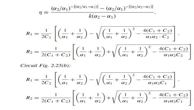
As far as
inductances are concerned, a general rule for the necessary critical damping of
single-stage or – with less accuracy of multistage generators can easily be
demonstrated . If individual inductances L1, L2 are considered within the
discharge circuit as indicated in Fig. 3.22(a), a second order differential
equation determines the output voltage across the load capacitance C2. However,
such an equivalent circuit cannot be exact, as additional circuitsrelated to
stray capacitances are not taken into account. Thus we may only combine the
total inductance within the C1 –C2 circuit to single inductance L, as shown in
Fig. 3.22 (b), and neglect the positions of the tail resistors, which have no
big influence. This reduces the circuit to a simple damped series resonant
circuit, and the critical resistance R D R1 for the circuit to
beNon-oscillatory is given by the well-known equation
This equation
is in general suitable for predicting the limiting values for the front
resistor R1. The extremely tedious analytical analysis of circuits containing
individual inductances is shown elsewhere. Computer programs for transients may
also be used to find the origin of oscillations, although it is difficult to
identify good equivalent circuits.
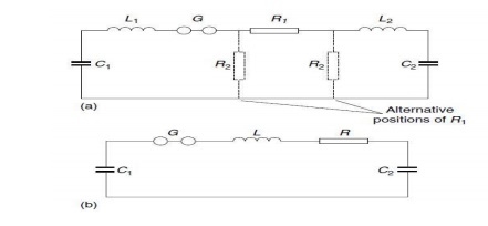
Figure:
3.22 Simplified circuit of impulse generator and load. Circuit showing
alternative positions of the wave tail control resistance. (b) Circuit for
calculation of wave front oscillations
Related Topics