Chapter: VLSI Design : CMOS Technology
Important Short Questions and Answers: VLSI Design - CMOS Technology
1. Define Threshold voltage
The
threshold voltage VT for a MOS transistor can be defined as the voltage between
the gate and the source terminals below which the drain to source current
effectively drops to zero.
2. Define body effect or substrate bias effect.
The
threshold voltage VT is not a constant with respect to the voltage difference
between the substrate and the source of the MOS transistor. This effect is
called the body effect or substrate bias effect.
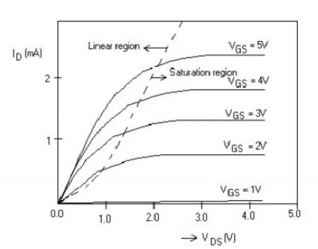
3. Give the different modes of operation of MOS
transistor
Cut off
mode Linear mode Saturation mode
4.
What are
the different regions of operation of a MOS transistor?
a. Cut off region
Here the
current flow is essentially zero (accumulation mode)
b. Linear region
It is
also called weak inversion region where the drain current is dependent on the
gate and the drain voltage w. r. to the substrate.
c. Saturation region
Channel
is strongly inverted and the drain current flow is ideally independent of the
drain-source voltage (strong-inversion region).
5. Give the expressions for drain current for
different modes of operation of
MOS transistor.
a. Cut off
region ID =0
b. Linear
region
ID = kn
[(VGS – VT) VDS – VDS2/2]
c.
Saturation region
ID = (kn
/2) (VGS – VT)2
6. Plot the current-voltage characteristics of a
nMOS transistor.
7. Define accumulation mode.
The
initial distribution of mobile positive holes in a p type silicon substrate of
a mos transistor for a voltage much less than the threshold voltage
8. What are the secondary effects of MOS transistor?
a.
Threshold voltage variations
b.
Source to drain resistance
c.
Variation in I-V characteristics
d.
Subthreshold conduction
e.
CMOS latchup
9. What is CMOS latchup? How it can be prevented?
The MOS
technology contains a number of intrinsic bipolar transistors.These are
especially troublesome in CMOS processes, where the combination of wells and
subtrates results in the formation of p-n-p-n structures. Triggering these
thyristor like devices leads to a shorting of VDD & VSS lines, usually
resulting in a destruction of the chip.
10.The remedies for the latch-up problem include:
(i) an
increase in substrate doping levels with a consequent drop in the value of
Rpsubs.
(ii) reducing
Rnwell by control of fabrication parameters and ensuring a low contact
resistance to VDD.
(iii) by
introducing guard rings.
11.
What are
the different fabrication processes available to CMOS technology?
a.
p-well process
b.
n-well process
c.
Twin-tub process
d.
Silicon On Insulator (SOI) / Silicon On Sapphire
(SOS) process
12.
What is
intrinsic and extrinsic semiconductor?
The pure
silicon is known as Intrinsic Semiconductor. When impurity is added with pure
silicon, it is electrical properties are varied. This is known as Extrinsic
semiconductor.
13. What are the steps involved in manufacturing of
IC?
i. wafer preparation
ii.
Epitaxial growth
iii. Oxidation
iv. photo
lithography
v.
Diffusion and Ion Implantation
vi. Isolation
vii. Metallization
14. What is meant by ‘ epitaxy ’ ?
Epitaxy
means arranging atoms in single crystal fashion upon a single crystal
substrate.
15.
what are
the process involved in photo lithography?
i.
making process
ii.
photo etching process
these are
important process involved in photolithography.
16. what is the purpose of masking in fabrication
of IC?
Masking
is used to identify the place in which Ion Implantion should not be occurred.
17. what are the materials used for masking?
Photo
resist, Sio2, SiN, poly Silicon.
18.what are the types of etching ?
Wet
etching and dry etching are the types of photo etching.
19. what is diffusion process ? what are doping
impurities?
Diffusion
is a process in which impurities are diffused in to the silicon chip at 10000C
temperature. B2O3 and P2O5 are used
as impurities.
20. what is isolation?
It is a
process used to provide electrical isolation between different components and
interconnections.
21. what are the various CMOS technologies?
Various
CMOS technologies are
i.
n-well process or n-tub process
ii.
p-well process or p-tub process
iii. twin-tub
process
iv.
Silicon on Insulator (SOI) process.
22. what is channel stop implantation?
In n-well
fabrication, n-well is protected with resist material. Because, it should not
be affected by Boron implantation. The boron is implanexcept n-well. It is done
using photoresist mask. This type of implantation is known as channel
implantation.
23. what is LOCS?
LOCOS
means Local Oxidation Of Silicon. This is one type of oxide construction.
24. what is SWAMI?
SWAMI
means Side Wall Masked Isolation. It is used to reduce bird’s beak effect.
25. what is LDD?
LDD means
Light Doped Drain Structures. It is used for implantation of n- in n-well
process.
26. what is twin-tub process? Why it is called so?
Twin-tub
process is one of the CMOS technology. There are two wells are available in
this process. The other name of well is tub. So, because of these two tubs,
this process is known as twin-tub process.
Related Topics