Chapter: VLSI Design : Combinational and Sequential Circuit Design
Important Short Questions and Answers: Combinational and Sequential Circuit Design
1. What are the static properties of complementary
CMOS Gates?
a.
They exhibit rails-to-rail swing with VOH = VDD and
VOL = GND.
b.
The circuits have no static power dissipation,
since the circuits are designed such that the pull-down and pull-up networks
are mutually exclusive.
c.
The analysis of the DC voltage transfer
characteristics and the noise margins is more complicated than for the
inverter, as these parameters depend upon the data input patterns applied to
the gate.
2. Draw the equivalent RC model for a two-input
NAND gate.
3. What are the major limitations associated with
complementary CMOS gate? a. The number of transistors required to implement
an N fan-in gate is 2N. This can result
in a significantly large implementation area.
b. The
propagation delay of a complementary CMOS gate deteriorates rapidly as a
function of the fan-in.
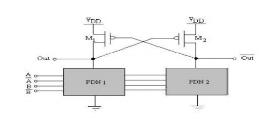
4. What is meant by ratioed logic?
In
ratioed logic, a gate consists of an nMOS pull-down network that realizes the
logic function and a simple load device, which replace the entire pull-up
network. A ratioed logic which uses a grounded pMOS load is referred to as a
pseudo-nMOS gate
5. What is true single phase clocked register?
The True
single-phase clocked register (TSPCR) uses a single clock, CLK. For the
positive latch, when CLK is high, the latch is in the transparent mode and
corresponds to two cascaded inverters; the latch is non-inverting, and
propagates the input to the output. On the other hand, when CLK=0, both
inverters are disabled, and the latch is in the hold mode.
6. Define a tally circuit.
A tally
circuit counts the number of inputs that are high and outputs the answer. If
there are N inputs there are N +1 possible outputs, corresponding to 0, 1, 2,
…. N inputs that are high.
7. Give the NAND-GATE
8. Give the 3 INPUT NAND-GATE
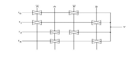
9. Draw the CMOS implementation of 4-to-1 MUX
using transmission gates .
10.
What are
the various mo deling used in Verilog?
1. Gate-level
modeling
2. Data-flow
modeling
3. Switch-level
modeling
4. Behavioral
modeling
11.
What is
the structural ga te-level modeling?
Structural
modeling deescribes a digital logic networks in terms of t he components that
make up the system. Gate-lev el modeling is based on using primitive logic
gates and specifying how they are wired together.
12.What is Switch-level mod eling?
Verilog
allows switch-level modeling that is based on the behavior of MOSFETs. Digital
circuits at the MOS-transistor level are described using the MOSFET switches.
13.
What are
the types of programmable device?
Programmable
logic structure
Programmable
Interconnect
Reprogrammable
gate arry
14.
What is
CLB?
CLB means
Configurable Log ic Block.
15.What are the two types of MOSFET?
Two types
of MOSET are n -channel MOSET and p-channel MOSFET. These are known as n-MOS
and p-MOS.
16.which MOS can pass logic 1 and logic 0 strongly?
p-MOS can
pass strong logic 1
n-MOS can
pass strong logic 0
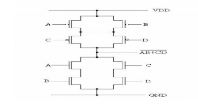
17. What is AOI logic function?
AND OR
Invert logic funct ion (AOI) implements operation in the or der of AND, OR, NOT
operations. So this logic function is known as AOI logic function.
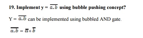
18. What is bubble pushing?
According
to De Morgan’s la ws,
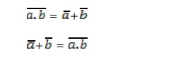
So NAND
gate may be draw n as bubbled OR gate. Bubbles are introduce d in the input
side. This concept is known as bubble pushing.
20. What is OAI 221 Gate?
OAI 221,
here 221 refers to n umber of inputs in each section.
21.
Write the
features of CM OS Domino Logic?
ü These
structures occup y small area compared with conventional lo gic structure.
ü Parasitic
capacitance is to be small to increase the speed.
ü Each gate
can make o ne ‘logic 1’ to ‘logic 0’ transition.
22.
What are
the tally circuits?
ü Tally
circuits one of th e applications of the pass transistor logic.
ü It is
used to count the number of inputs which are high and the outp ut is produced.
23.
What are
the various for ms of inverter based CMOS logic?
i.
Pseudo N-MOS logic
ii.
Dynamic C-MOS logic
iii. Clocked
C-MOS logic
iv. C-MOS
domino logic
v.
n-p C-MOS logic
24.
What is
PIP in XILINIX?
PIP means
Programmable Int erconnect Point in XILINIX.
25. What are the advantagess and disadvantages of
PLA?
Advantages of PLA
ü Simplicity
ü Small
size
Disadvantages of PLA
ü Speed problem occur ( pull-ups may become slow on large terms )
Related Topics