Chapter: VLSI Design : Circuit Characterization and Simulation
Important Short Questions and Answers: Circuit Characterization and Simulation
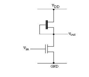
1. Draw the circuit of a nMOS inverter.
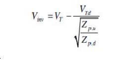
2. Give the expression for pull-up to pull-down
ratio ( Zpu/Zpd) for an nMOS inverter driven by another nMOS
inverter.
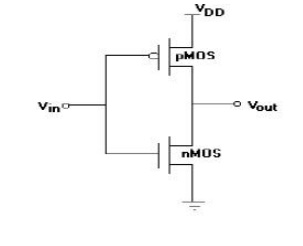
3. Draw the circuit of a CMOS inverter.
4. What are the advantages of CMOS inverter over the
other inverter configurations?
a. The
steady state power dissipation of the CMOS inverter circuit is negligible.
b. The voltage transfer
characteristic (VTC) exhibits a full output voltage wing between 0V and VDD. This results in high noise
margin.
5. What are stick diagrams?
Stick
diagrams are used to convey layer information through the use of a color code.
A stick diagram is a cartoon of a chip layout. They are not exact models of
layout. The stick diagram represents the rectangles with lines which represent
wires and component symbols.
6. What are the different color codes used for single
poly silicon nMOS technology?
·
n-diffusion (n-diff.) and other thinoxide regions
-green
·
Polysilicon (poly.) - red
·
Metal 1 (metal) - blue Implant - yellow
·
Contacts - black or brown (buried)
7. What are design rules?
Design
rules are the communication link between the designer specifying requirements
and the fabricator who materializes them. Design rules are used to produce
workable mask layouts from which the various layers in silicon will be formed
or patterned.
8. Define a superbuffer.
A
superbuffer is a symmetric inverting or noninverting gate that can supply or
remove large currents and switch large capacitive loads faster than a standard
inverter.
9.What are BiCMOS Gates?
When
bipolar and MOS technology are merged, the resulting circuits are referred to
as biCMOS circuits. High gain vertical npn transistors with their collectors
tied to the positive rail, and medium-gain lateral npn transistors are both
compatible with conventional CMOS processing. BiCMOS gates can be used to
improve the performance of line drivers and sense amplifiers.
10. what is the special feature of twin-tub
process?
In
twin-tub process, threshold voltage, body effect n and p devices are
independently optimized.
11. what are the advantage of twin-tub process?
Advantages
of twin-tub process are
i.
Separate optimized wells are available.
ii.
Balance performance is obtained for n and p
transistors.
12. what is SOI? What is the material used as
Insulator?
SOI means
Silicon-on-Insulator. In this process, Sapphire or SiO2 is used as
insulator.
13. what are the various etching process used in
SOI process?
Various
etching process used in SOI are
i.
Isotropic etching process.
ii.
Anisotropic etching process.
iii. Preferential
etching process.
14.
what are
the advantages and disadvantages 0f SOI process? Advantages of SOI process
i.
There is no well formation in this process.
ii.
There is no field-Inversion problem.
iii. There is
no body effect problem.
Disadvantages of SOI process
i.
It is very difficult to protect inputs in this
process.
ii.
Device gain is low.
iii. The
coupling capacitance between wires always exist.
15.
what are
the possible modes in nMOS enhancement transistor?
i.
accumulation mode
ii.
depletion mode
ii.
Inversion mode
16.
In
saturation region, what are the factors that affect Ids?
i.
distancebetween source and drain.
ii.
channel width
iii. Threshold
oltage
iv. thickness
of oxide layer
v.
dielectric constant of gate insulator
vi. Carrier
mobility.
17.What is Body effect?
The
threshold voltage VT is not a constant w. r. to the voltage difference between
the substrate and the source of MOS transistor. This effect is called
substrate-bias effect or body effect.
18.What is Channel-length modulation?
The
current between drain and source terminals is constant and independent of the
applied voltage over the terminals. This is not entirely correct. The effective
length of the conductive channel is actually modulated by the applied VDS,
increasing VDS causes the depletion region at the drain junction to grow,
reducing the length of the effective channel.
19. Define Threshold voltage in CMOS?
The
Threshold voltage, VT for a MOS transistor can be defined as the
voltage applied between the gate and the source of the MOS transistor below
which the drain to source current, IDS effectively drops to zero.
20. Define Rise time
Rise
time, tr is the time taken for a waveform to rise from 10% to 90% of its steady-state
value.
21. Define Fall time
Fall time, tf is the time taken
for a waveform to fall from 90% to 10% of its steady-state value.
22. Define Delay time
Delay
time, td is the time difference between input transition (50%) and the 50%
output level. This is the time taken for a logic transition to pass from input
to output.
23. What are two components of Power dissipation?
There are
two components that establish the amount of power dissipated in a CMOS circuit.
These are:
i) Static
dissipation due to leakage current or other current drawn continuously from the
power supply.
ii) Dynamic
dissipation due to - Switching transient current – Charging and discharging of
load capacitances.
24. Give some of the important CAD tools.
Some of
the important CAD tools are:
i) Layout
editors
ii) Design
Rule checkers (DRC)
iii) Circuit
extraction
Related Topics