Chapter: Microprocessor and Microcontroller
INTEL 8255: (Programmable Peripheral Interface)
INTEL 8255: (Programmable Peripheral Interface)
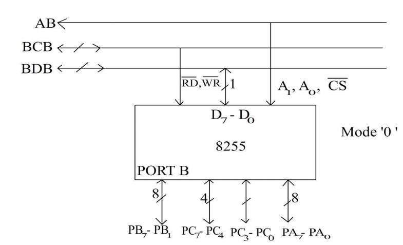
The 8255A is a general purpose programmable I/O
device designed for use with Intel microprocessors. It consists of three 8-bit
bidirectional I/O ports (24I/O lines) that can be configured to meet different
system I/O needs. The three ports are PORT A, PORT B & PORT C. Port A
contains one 8-bit output latch/buffer and one 8-bit input buffer. Port B is
same as PORT A or PORT B. However, PORT C can be split into two parts PORT C
lower (PC0-PC3) and PORT C upper (PC7-PC4)
by the control word. The three ports are divided in two groups Group A (PORT A
and upper PORT C) Group B (PORT B and lower PORT C). The two groups can be
programmed in three different modes. In the first mode (mode 0), each group may
be programmed in either input mode or output mode (PORT A, PORT B, PORT C
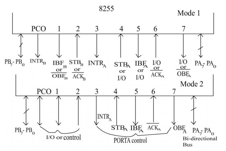
lower, PORT C upper). In mode 1, the second’s mode, each group may be
programmed to have 8-lines of input or output (PORT A or PORT B) of the
remaining 4-lines (PORT C lower or PORT C upper) 3-lines are used for hand
shaking and interrupt control signals. The third mode of operation (mode 2) is
a bidirectional bus mode which uses 8-line (PORT A only for a bidirectional bus
and five lines (PORT C upper 4 lines and borrowing one from other group) for
handshaking.
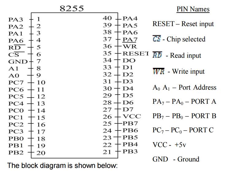
The 8255 is contained in a 40-pin package, whose
pin out is shown below:
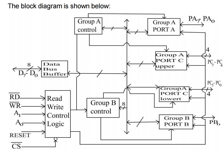
Functional Description:
This support chip is a general purpose I/O
component to interface peripheral equipment to the microcomputer system bus. It
is programmed by the system software so that normally no external logic is
necessary to interface peripheral devices or structures.
Data Bus Buffer:
It is a tri-state 8-bit buffer used to interface
the chip to the system data bus. Data is transmitted or received by the buffer
upon execution of input or output instructions by the CPU. Control words and
status information are also transferred through the data bus buffer. The data
lines are connected to BDB of p
Read/Write and logic control:
The function of this block is to control the
internal operation of the device and to control the transfer of data and
control or status words. It accepts inputs from the CPU address and control
buses and in turn issues command to both the control groups.
 ^(CS) Chip Select:
A low on this input selects the chip and enables
the communication between the 8255 A & the CPU. It is connected to the
output of address decode circuitry to select the device when it  ^(RD)
(Read). A low on this input enables the 8255 to send the data or status
information to the CPU on the data bus.
^(RD)
(Read). A low on this input enables the 8255 to send the data or status
information to the CPU on the data bus.
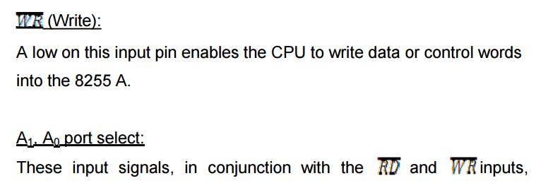
control the selection of one of the three ports
or the control word registers. They are normally connected to the least
significant bits of the address bus (A0 and A1).
Following Table gives the basic operation,
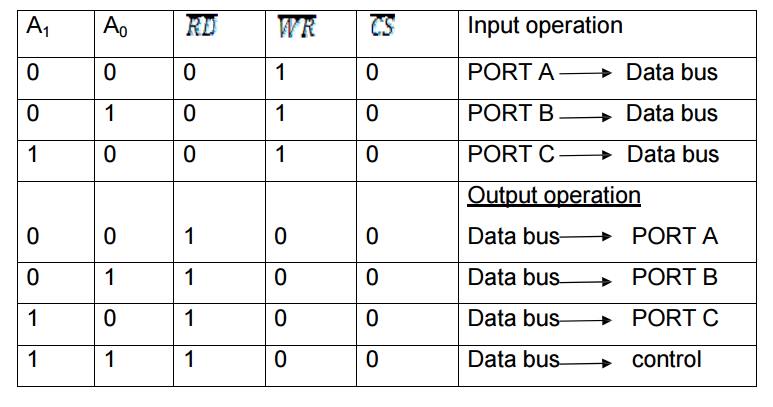
All other states put data bus into
tri-state/illegal condition.
RESET:
A high on this input pin clears the control
register and all ports (A, B & C) are initialized to input mode. This is
connected to RESET OUT of 8255. This is done to prevent destruction of
circuitry connected to port lines. If port lines are initialized as output
after a power up or reset, the port might try to output into the output of a
device connected to same inputs might destroy one or both of them.
PORTs A, B and C:
The 8255A contains three 8-bit ports (A, B and
C). All can be configured in a variety of functional characteristic by the
system software.
PORTA:
One 8-bit data output latch/buffer and one 8-bit
data input latch.
PORT B:
One 8-bit data output latch/buffer and one 8-bit
data input buffer.
PORT C:
One 8-bit data output latch/buffer and one 8-bit
data input buffer (no latch for input). This port can be divided into two 4-bit
ports under the mode control. Each 4-bit port contains a 4-bit latch and it can
be used for the control signal outputs and status signals inputs in conjunction
with ports A and B.
Group A & Group B control:
The functional configuration of each port is
programmed by the system software. The control words outputted by the CPU configure
the associated ports of the each of the two groups. Each control block accepts
command from Read/Write content logic receives control words from the internal
data bus and issues proper commands to its associated ports.
Control Group A – Port A & Port C upper
Control Group B – Port B & Port C lower
The control word register can only be written
into No read operation if the control word register is allowed.
Operation Description:
Mode selection:
There are three basic modes of operation that can
be selected by the system software.
Mode 0: Basic Input/output Mode 1: Strobes
Input/output Mode 2: Bi-direction bus.
When the reset input goes HIGH all poets are set
to mode’0’ as input which means all 24 lines are in high impedance state and
can be used as normal input. After the reset is removed the 8255A remains in
the input mode with no additional initialization. During the execution of the
program any of the other modes may be selected using a single output
instruction.
The modes for PORT A & PORT B can be
separately defined, while PORT C is divided into two portions as required by
the PORT A and PORT B definitions. The ports are thus divided into two groups
Group A & Group B. All the output register, including the status flip-flop
will be reset whenever the mode is changed. Modes of the two group may be
combined for any desired I/O operation e.g. Group A in mode ‘1’ and group B in
mode ‘0’.
The basic mode definitions with bus interface
and the mode definition format are given in fig (a) & (b),
Related Topics