Chapter: Linear Integrated Circuits : Basics of Operational Amplifiers
General Operational Amplifier stages and internal circuit diagrams of IC 741
General
Operational Amplifier stages and internal circuit diagrams of IC 741
An
operational amplifier generally consists of three stages, namely
1.
A
differential amplifier
2.
Additional
amplifier stages to provide the required voltage gain and dc level shifting.
3.
An
emitter-follower or source follower output stage to provide current gain and
low output resistance.
A
low-frequency or dc gain of approximately 104 is desired for a general purpose
op-amp and hence, the use of active load is preferred in the internal circuitry
of op-amp.
The
output voltage is required to be at ground, when the differential input
voltages are zero, and this necessitates the use of dual polarity supply
voltage. Since the output resistance of op-amp is required to be low, a
complementary push-pull emitter – follower or source follower output stage is
employed. Moreover, as the input bias currents are to be very small of the
order of pico amperes, an FET input stage is normally preferred.
Input stage:
The
input differential amplifier stage uses p-channel JFETs M1 and M2.
It employs a three-transistor active load formed by Q3, Q4,
and Q5. The bias current for the stage is provided by a
two-transistor current source using PNP transistors Q6 and Q7.
Resistor R1 increases the o utput resistance seen looking into the
collector of Q4 as indicated by R04. This is necessary to
provide bias current stability against the transistor parameter variations.
Resistor R2 establishes a definite bias current through Q5.
A single ended output is taken out at the collector of Q4.
MOSFET‘s
are used in place of JFETs with additional devices in the circuit to prevent
any damage for the gate oxide due to electrostatic discharges.
Gain stage:
The
second stage or the gain stage uses Darlington transistor pair formed by Q8
and Q9 as shown in figure. The transistor Q8 is connected as an
emitter follower, providing large input resistance.
Therefore,
it minimizes the loading effect on the input differential amplifier stage. The
transistor Q9 provides an additional gain and Q10 acts as
an active load for this stage. The current mirror formed by Q7 and Q10
establishes the bias current for Q9. The VBE drop across Q9
and drop across R5 constitute the voltage drop across R4,
and this voltage sets the current through Q8. It can be set to a
small value, such that the base current of Q8 also is very less.
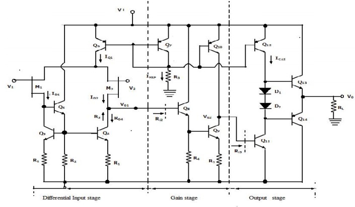
Output stage:
The
final stage of the op-amp is a class AB complementary push-pull output stage. Q11
is an emitter follower, providing a large input resistance for minimizing the
loading effects on the gain stage. Bias current for Q11 is provided
by the current mirror formed by Q7 and Q12, through Q13
and Q14 for minimizing the cross over distortion. Transistors can
also be used in place of the two diodes.
The
overall voltage gain AV of the op-amp is the product of voltage gain of each
stage as given by AV=|Ad| |A2||A3|
Where
Ad is the gain of the differential amplifier stage, A2 is
the gain of the second gain stage and A3 is the gain of the output
stage.
IC 741 Bipolar operational amplifier:
The
IC 741 produced since 1966 by several manufactures is a widely used general
purpose operational amplifier. Figure shows that equivalent circuit of the 741
op-amp, divided into various individual stages. The op-amp circuit consists of
three stages.
1. The input differential amplifier
2. The gain stage
3. the output stage.
A
bias circuit is used to establish the bias current for whole of the circuit in
the IC. The op-amp is supplied with positive and negative supply
voltages of value ± 15V and the supply voltages as low as ±5V can also be used.
Bias Circuit:
The
reference bias current IREF for the 741 circuit is established by the bias
circuit consisting of two diodes-connected transistors Q11 and Q12
and resistor R5. The Widlar current source formed by Q11,
Q10 and R4 provide bias current for the differential
amplifier stage at the collector of Q10. Transistors Q8
and Q9 form another current mirror providing bias current for the
differential amplifier. The reference bias current IREF also provides mirrored
and proportional current at the collector of the double –collector lateral PNP
transistor Q13. The transistor Q13 and Q12
thus form a two-output current mirror with Q13A providing bias
current for output stage and Q13B providing bias current for Q17.
The transistor Q18 and Q19 provide dc bias for the output
stage. Formed by Q14 and Q20 and they establish two VBE
drops of potential difference between the bases of Q14 and Q18.
Input stage:
The
input differential amplifier stage consists of transistors Q1 through Q7 with
biasing provided by Q8 through Q12. The transistor Q1 and Q2 form emitter –
followers contributing to high differential input resistance, and whose output
currents are inputs to the common base amplifier using Q3 and Q4 which offers a
large voltage gain. The transistors Q5, Q6 and Q7 along with resistors R1, R2
and R3 from the active load for input stage. The single-ended output is
available at the collector of Q6. The two null terminals in the input stage
facilitate the null adjustment. The lateral PNP transistors Q3 and Q4 provide
additional protection against voltage breakdown conditions. The emitter-base
junction Q3 and Q4 have higher emitter-base breakdown voltages of about 50V.
Therefore, placing PNP transistors in series with NPN transistors provide
protection against accidental shorting of supply to the input terminals.
Gain Stage:
The
Second or the gain stage consists of transistors Q16 and Q17,
with Q16 acting as an emitter – follower for achieving high input
resistance. The transistor Q17 operates in common emitter configuration
with its collector voltage applied as input to the output stage. Level shifting
is done for this signal at this stage.
Internal
compensation through Miller compensation technique is achieved using the
feedback capacitor C1 connected between the output and input terminals of the
gain stage.
Output stage:
The
output stage is a class AB circuit consisting of complementary emitter follower
transistor pair Q14 and Q20. Hence, they provide an
effective loss output resistance and current gain. The output of the gain stage
is connected at the base of Q22, which is connected as an emitter
follower providing a very high input resistance, and it offers no appreciable
loading effect on the gain stage. It is biased by transistor Q13A
which also drives Q18 and Q19, that are used for establishing a quiescent bias
current in the output transistors Q14 and Q20.
Related Topics