Functional block diagram, Output waveform, Pin description, Important features, Parameters - Function Generator IC 8038 | Linear Integrated Circuits : Waveform Generators and Special Function ICs
Chapter: Linear Integrated Circuits : Waveform Generators and Special Function ICs
Function Generator IC 8038
Function
Generator IC 8038:
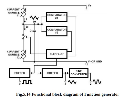
It
consists of two current sources, two comparators, two buffers, one FF and a
sine wave converter.
Pin description:
·
Pin
1 & Pin 12: Sine wave adjusts:
The
distortion in the sine wave output can be reduced by adjusting the 100KΩ pots connected
between pin12 & pin11 and between pin 1 & 6.
·
Pin
2 Sine Wave Output:
Sine
wave output is available at this pin. The amplitude of this sine wave is 0.22
Vcc. Where ± 5V ≤ Vcc ≤ ± 15 V.
·
Pin
3 Triangular Wave output:
Triangular
wave is available at this pin. The amplitude of the triangular wave is 0.33Vcc.
Where
± 5V ≤ Vcc ≤ ± 15 V.
·
Pin
4 & Pin 5 Duty cycle / Frequency adjust:
The
symmetry of all the output wave forms & 50% duty cycle for the square wave
output is adjusted by the external resistors connected from Vcc to pin 4. These
external resistors & capacitors at pin 10 will decide the frequency of the
output wave forms.
·
Pin
6 + Vcc:
Positive
supply voltage the value of which is between 10 & 30V is applied to this
pin.
·
Pin
7 : FM Bias:
This
pin along with pin no8 is used to TEST the IC 8038.
·
Pin9
: Square Wave Output:
A
square wave output is available at this pin. It is an open collector output so
that this pin
can
be connected through the load to different power supply voltages. This
arrangement is very useful in making the square wave output.
·
Pin
10 : Timing Capacitors:
The
external capacitor C connected to this pin will decide the output frequency
along with the resistors connected to pin 4 & 5.
·
Pin
11 : -VEE or Ground:
If
a single polarity supply is to be used then this pin is connected to supply
ground & if (±) supply voltages are to be used then (-) supply is connected
to this pin.
·
Pin
13 & Pin 14: NC (No Connection)
Important features of IC 8038:
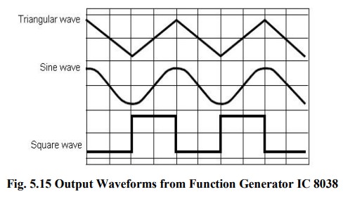
1. All the outputs are simultaneously available.
2. Frequency range : 0.001Hz to 500kHz
3. Low distortion in the output wave forms.
4. Low frequency drifts due to change in
temperature.
5. Easy to use.
Parameters:
(i) Frequency of the output wave form:
The
output frequency dependent on the values of resistors R1 & R2 along with
the external capacitor C connected at pin 10.
If
RA= RB = R & if RC is adjusted for 50% duty cycle then f0= 0.3/RC; RA = R1,
RB =
R3, RC= R2.
(ii) Duty cycle / Frequency Adjust : (Pin 4 &
5):
Duty
cycle as well as the frequency of the output wave form can be adjusted by
external resistors at pin 4 & 5.
The
values of resistors RA & RB connected between Vcc pin 4 & 5
respectively along
with
the capacitor connected at pin 10 decide the frequency of the wave form. The
values of RA & RB should be in the range of 1kΩ to 1MΩ.
(iii)FM
Bias:
• The FM Bias input (pin7) corresponds to the junction of resistors R1 & R2.
• The voltage Vin is the voltage between Vcc
& pin8 and it decides the output frequency.
• The output frequency is proportional to Vin
as given by the following expression.
For
RA = RB (50% duty cycle).
f0=
5 Vin/CRAVcc ; where C is the timing capacitor.
·
With
pin 7 & 8 connected to each other the output frequency is given by f0=
0.3/RC where R = RA = RB for 50% duty cycle.
·
This
is because M Sweep input (pin 8):
• Vin=R1Vcc/R1+R2
• This input should be connected to pin 7, if
we want a constant output frequency.
• But if the output frequency is supposed to
vary, then a variable dc voltage should be applied to this pin.
• The voltage between Vcc & pin 8 is
called Vin and it decides the output frequency as,
f0=1.5
Vin/CRAVCC
A
potentiometer can be connected to this pin to obtain the required variable
voltage required to change the output frequency.
Related Topics