Chapter: Digital Principles and System Design : Boolean Algebra and Logic Gates
Digital Logic Gates
DIGITAL LOGIC GATES
A logic gate is an electronic circuit/device which makes the logical decisions. To arrive at this decisions, the most common logic gates used are OR, AND, NOT, NAND, and NOR gates. The NAND and NOR gates are called universal gates. The exclusive-OR gate is another logic gate which can be constructed using AND, OR and NOT gate.
Logic gates have one or more inputs and only one output. The output is active only for certain input combinations. Logic gates are the building blocks of any digital circuit. Logic gates are also called switches. With the advent of integrated circuits, switches have been replaced by TTL (Transistor Transistor Logic) circuits and CMOS circuits. Here I give example circuits on how to construct simples gates.
•AND
•OR
•NOT
•BUF
•NAND
•NOR
•XOR
•XNOR
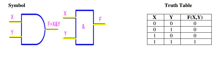
AND Gate
The AND gate performs logical multiplication, commonly known as AND function. The AND gate has two or more inputs and single output. The output of AND gate is HIGH only when all its inputs are HIGH (i.e. even if one input is LOW, Output will be LOW).
If X and Y are two inputs, then output F can be represented mathematically as F = X.Y, Here dot (.) denotes the AND operation. Truth table and symbol of the AND gate is shown in the figure below.
Two input AND gate using "diode-resistor" logic is shown in figure below, where X, Y are inputs and F is the output.
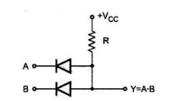
If X = 0 and Y = 0, then both diodes D1 and D2 are forward biased and thus both diodes conduct and pull F low.
If X = 0 and Y = 1, D2 is reverse biased, thus does not conduct. But D1 is forward biased, thus conducts and thus pulls F low.
If X = 1 and Y = 0, D1 is reverse biased, thus does not conduct. But D2 is forward biased, thus conducts and thus pulls F low.
If X = 1 and Y = 1, then both diodes D1 and D2 are reverse biased and thus both the diodes are in cut-off and thus there is no drop in voltage at F. Thus F is HIGH.
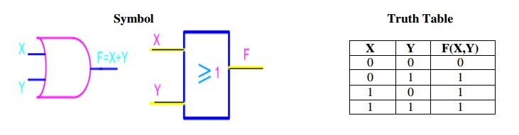
OR Gate
The OR gate performs logical addition, commonly known as OR function. The OR gate has two or more inputs and single output. The output of OR gate is HIGH only when any one of its inputs are HIGH (i.e. even if one input is HIGH, Output will be HIGH).
If X and Y are two inputs, then output F can be represented mathematically as F = X+Y. Here plus sign (+) denotes the OR operation. Truth table and symbol of the OR gate is shown in the figure below.
Two input OR gate using "diode-resistor" logic is shown in figure below, where X, Y are inputs and F is the output.
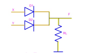
If X = 0 and Y = 0, then both diodes D1 and D2 are reverse biased and thus both the diodes are in cut-off and thus F is low.
If X = 0 and Y = 1, D1 is reverse biased, thus does not conduct. But D2 is forward biased, thus conducts and thus pulling F to HIGH.
If X = 1 and Y = 0, D2 is reverse biased, thus does not conduct. But D1 is forward biased, thus conducts and thus pulling F to HIGH.
If X = 1 and Y = 1, then both diodes D1 and D2 are forward biased and thus both the diodes conduct and thus F is HIGH.
NOT Gate
The NOT gate performs the basic logical function called inversion or complementation. NOT gate is also called inverter. The purpose of this gate is to convert one logic level into the opposite logic level. It has one input and one output. When a HIGH level is applied to an inverter, a LOW level appears on its output and vice versa.
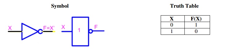
If X is the input, then output F can be represented mathematically as F = X', Here apostrophe (') denotes the NOT (inversion) operation. There are a couple of other ways to represent inversion, F= !X, here ! represents inversion. Truth table and NOT gate symbol is shown in the figure below.
NOT gate using "transistor-resistor" logic is shown in the figure below, where X is the input and F is the output.
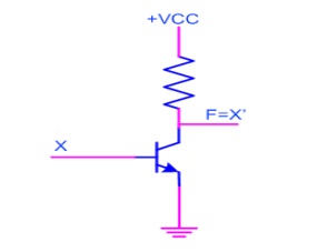
When X = 1, The transistor input pin 1 is HIGH, this produces the forward bias across the emitter base junction and so the transistor conducts. As the collector current flows, the voltage drop across RL increases and hence F is LOW.
When X = 0, the transistor input pin 2 is LOW: this produces no bias voltage across the transistor base emitter junction. Thus Voltage at F is HIGH.
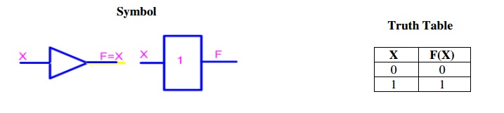
BUF Gate
Buffer or BUF is also a gate with the exception that it does not perform any logical operation on its input. Buffers just pass input to output. Buffers are used to increase the drive strength or sometime just to introduce delay. We will look at this in detail later.
If X is the input, then output F can be represented mathematically as F = X. Truth table and symbol of the Buffer gate is shown in the figure below.
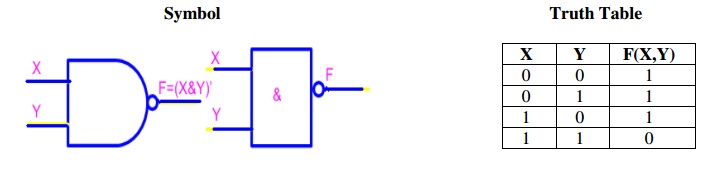
NAND Gate
NAND gate is a cascade of AND gate and NOT gate, as shown in the figure below. It has two or more inputs and only one output. The output of NAND gate is HIGH when any one of its input is LOW (i.e. even if one input is LOW, Output will be HIGH).
If X and Y are two inputs, then output F can be represented mathematically as F = (X.Y)', Here dot (.) denotes the AND operation and (') denotes inversion. Truth table and symbol of the N AND gate is shown in the figure below.
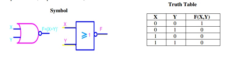
NOR Gate
NOR gate is a cascade of OR gate and NOT gate, as shown in the figure below. It has two or more inputs and only one output. The output of NOR gate is HIGH when any all its inputs are LOW (i.e. even if one input is HIGH, output will be LOW).
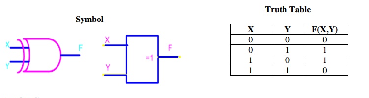
XOR Gate
An Exclusive-OR (XOR) gate is gate with two or three or more inputs and one output. The output of a two-input XOR gate assumes a HIGH state if one and only one input assumes a HIGH state. This is equivalent to saying that the output is HIGH if either input X or input Y is HIGH exclusively, and LOW when both are 1 or 0 simultaneously.
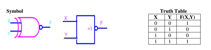
XNOR Gate
An Exclusive-NOR (XNOR) gate is gate with two or three or more inputs and one output. The output of a two-input XNOR gate assumes a HIGH state if all the inputs assumes same state. This is equivalent to saying that the output is HIGH if both input X and input Y is HIGH exclusively or same as input X and input Y is LOW exclusively, and LOW when both are not same.
Universal Gates
Universal gates are the ones which can be used for implementing any gate like AND, OR and NOT, or any combination of these basic gates; NAND and NOR gates are universal gates. But there are some rules that need to be followed when implementing NAND or NOR based gates.
Ref: 1) A.P Godse & D.A Godse “Digital Electronics”, Technical publications, Pune, Revised edition, 2008. Pg.No:3.1-3.17.
2) Morris Mano M. and Michael D. Ciletti, “Digital Design”, IVPearsonEdition,Education, 2008. Pg.No:57.
Related Topics