explanation with block diagram | Operational Amplifiers - Differential amplifier | Linear Integrated Circuits : Basics of Operational Amplifiers
Chapter: Linear Integrated Circuits : Basics of Operational Amplifiers
Differential amplifier
Differential
amplifier
The
function of a differential amplifier is to amplify the difference between two
signals. The need for differential amplifier arises in many physical
measurements where response from DC to many MHz of frequency is required. This
forms the basic input stage of an integrated amplifier.
The
basic differential amplifier has the following important properties of
·
Excellent
stability
·
High
versatility and
·
High
immunity to interference signals
The
differential amplifier as a building block of the op-amp has the advantages of
·
Lower
cost
·
Easier
fabrication as IC component and
·
closely
matched components.
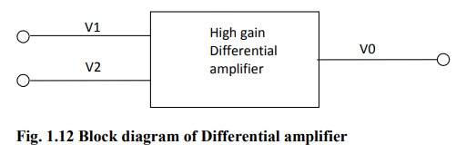
The
above figure shows the basic block diagram of a differential amplifier, with
two input terminals and one output terminal. The output signal of the
differential amplifier is proportional to the difference between the two input
signals.
V0
= Adm ( V1 – V2 )
If
V1 = V2, then the
output voltage is zero. A non-zero output voltage V0 is obtained when V1 and V2 are not equal.
The difference mode input voltage is defined as Vm = V1 – V2 and the common
mode input voltage is defined as
These
equation show that if V1 = V2,
then the differential mode input signal is zero and common mode input signal is
Vcm = V1 =V2.
Differential Amplifier with Active load:
Differential
amplifier is designed with active loads to increase the differential mode
voltage gain. The open circuit voltage gain of an op-amp is needed to be as
large as possible. This is got by cascading the gain stages which increase the
phase shift and the amplifier also becomes vulnerable to oscillations. The gain
can be increased by using large values of collector resistance. For such a
circuit, the voltage gain is given by
Adm
= gm RC
To
increase the gain the IC RC product must be made very large. However, there are
limitations in IC fabrication such as,
1.
A
large value of resistance needs a large chip area.
2.
For
large RC, the quiescent drop across the resistor increase and a large power
supply will be required to maintain a given operating current.
3.
Large
monolithic resistor introduces large parasitic capacitances which limits the frequency
response of the amplifier.
4.
for
linear operation of the differential pair, the devices should not be allowed to
enter into saturation. This limits the max input voltage that can be applied to
the bases of transistors Q1 and Q2 the base-collector junction
must be allowed to become forward-biased by more than 0.5V. The large value of
load resistance produces a large dc voltage drop (IEE / 2) RC,
so that the collector voltage will be VC=Vcc - (IEE/2) RC and it
will be substantially less than the supply voltage Vcc. This will reduce the
input voltage range of the differential amplifier. Due to the reasons cited
above, an active load is preferred in the differential amplifier
configurations.
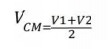
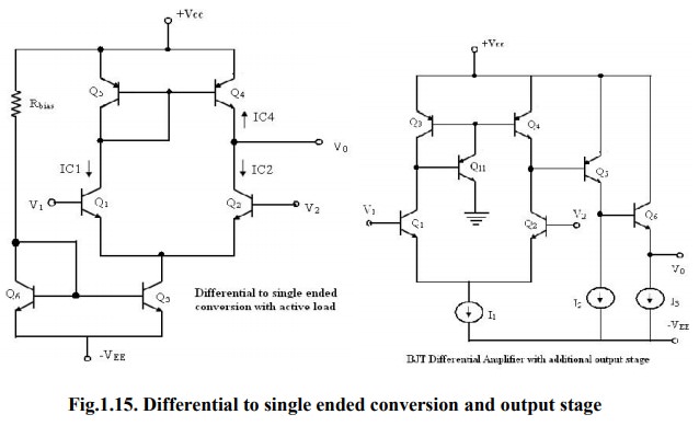
BJT Differential Amplifier using active loads:
A
simple active load circuit for a differential amplifier is the current mirror
active load as shown in figure. The active load comprises of transistors Q3
and Q4 with the transistor Q3 connected as a Diode with
its base and collector shorted. The circuit is shown to drive a load RL. When
an ac input voltage is applied to the differential amplifier, the various
currents of the circuit are given by IC4 = IC3 = IC1
= gmVid/2 where IC4 = IC3 due to current mirror action.
IC2
= - gmVid/2 .
We
know that the load current IL entering the next stage is IL= IC2-IC4
= - gmVid/2 - gmVid/2 = - gmVid
Then,
the output voltage from the differential= amplifier= is given by V0=
- ILRL = gm RLVid. The ac voltage
gain of the circuit is given by Av = v0/vid =
gmRL. The amplifier can amplify the differential input signals and
it provides single-ended output with a ground reference since the load RL
is connected to only one output terminal. This is made possible by the use of
the current mirror active load. The output resistance R0 of the circuit is that
offered by the parallel combination of transistors Q2 (NPN) and Q4
(PNP). It is given by Rr = r02 || r04.
Analysis of BJT differential amplifier with active load:
The
collector currents of all the transistors are equal.
IC1
= IC2 = IC3 =IC4 = IEE/2 .
The
Collector -emitter voltages of Q1 and Q2 are given by
VCE1-VCE2
=VC-VE=VCC - VEB-(-VEB)=
VCC
Eqn.
shows that, the offset is higher than that of a resistive loaded differential
amplifier A. This can be reduced by the use of emitter resistors for Q3
and Q4 , and a transistor Q5 in the current mirror load.
CMRR of the differential amplifier using active load:
The
differential amplifier using active load provides high voltage gain to the
differential input signal and a single – ended output that is referenced to the
ground is obtained. The differential amplifier which provides conversion for a
differential signal to a single ended signal is necessary in differential input
signal ended output amplifiers. The op-amp is one such circuit. The changes in
the common-mode signal of the bias current source. This induces a change in IC2
and an identical change in IC1. The change in IC1 will
then produce a change in the PNP load devices, and thereby a change in IC4,
which is the collector current Q4, The current IC4 is in
such a direction as to cancel the change in IC2. As a result of
this, any common mode input does not cause a change in output.
The
voltage gain of the differential amplifier is independent of the quiescent
current IEE. This makes it possible to use very small value of IEE
as low as 20μA, while still maintaining a large voltage gain. Small value of IEE
is preferred, since it results in a small value of bias current and a large
value for the input resistance. A limitation in choosing a small IEE
is, however, the fact that, it will result in a poor frequency response of the
amplifier.
When
a small value of bias current is required, the best approach is to use a JFET
or MOSFET differential amplifier that is operated at comparatively higher
values of IEE.
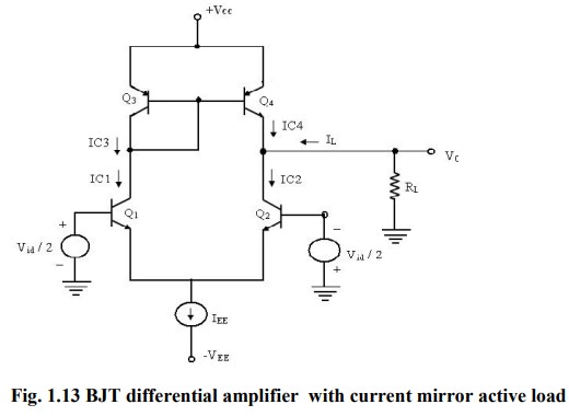
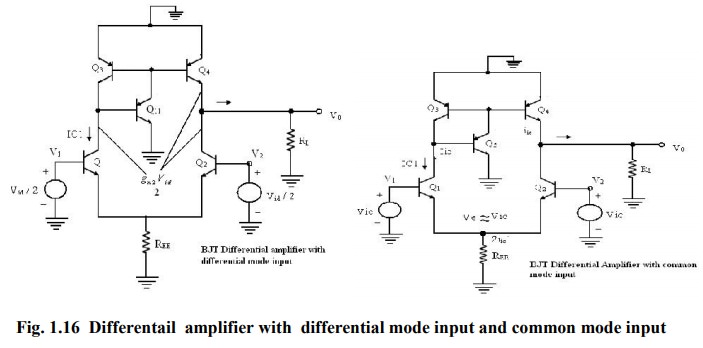
Differential Mode signal analysis:
The
ac analysis of the differential amplifier can be made using the circuit model
as shown below. The differential input transistor pair produces equal and
opposite currents whose amplitude us given by gm2 Vid /2 at the
collector of Q1 and Q2. The collector current Ic1
is fed by the transistor Q3 and it is mirrored at the output of Q4.
Therefore, the total current i0 flowing through the load resistor RL
is given by i0 = [2gm2Vid]/2 = gm2Vid.
Then the output voltage is v0
=i0RL – gm2RLvid and
the differential mode gain Ad of the differential amplifier is
This
current mirror provides a single ended output which has a voltage equal to the maximum
gain of the common emitter amplifier.
The
power of the current mirror can be increased by including additional common
collector stages at the o/p of the differential input stage. A bipolar
differential amplifier structure with additional stages is shown in figure. The
resistance at the output of the differential stage is now given by the parallel
combination of transistors Q2 and Q4 and the input
resistance is offered by Q5. Then, the equivalent resistance is
expressed by Req = ro2 || r04 || ri5 = ri5.
The
gain of the differential stage then becomes
Adm = gm2 Req
= gm2 ri5=βIC2/IC5 .
Related Topics