Chapter: Basic Electrical and Electronics Engineering : Digital Electronics
Data Latch
Data Latch
One of
the main disadvantages of the basic SR NAND Gate Bistable circuit is that the
indeterminate input condition of "SET" = logic "0" and
"RESET" = logic "0" is forbidden. That state will force
both outputs to be at logic "1", over-riding the feedback latching
action and whichever input goes to logic level "1" first will lose
control, while the other input still at logic "0" controls the
resulting state of the latch. In order to prevent this from happening an
inverter can be connected between the "SET" and the "RESET"
inputs to produce a D-Type Data Latch or
simply Data Latch as it is generally
called.
Data Latch Circuit
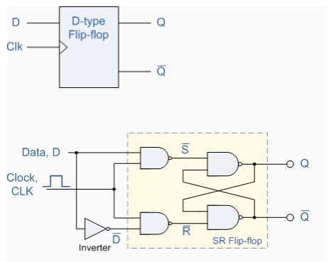
We
remember that the simple SR flip-flop requires two inputs, one to
"SET" the output and one to "RESET" the output. By
connecting an inverter (NOT gate) to the SR flip-flop we can "SET"
and "RESET" the flip-flop using just one input as now the two latch
inputs are complements of each other. This single input is called the
"DATA" input. If this data input is HIGH the flip-flop would be
"SET" and when it is LOW the flip-flop would be "RESET".
However, this would be rather pointless since the flip-flop's output would
always change on every data input. To avoid this an additional input called the
"CLOCK" or "ENABLE" input is used to isolate the data input
from the flip-flop after the desired data has been stored. This then forms the
basis of a Data Latch or
"D-Type latch".
The D-Type Latch will store and output
whatever logic level is applied to its data terminal so long as the clock input
is high. Once the clock input goes low the SET and RESET inputs of the
flip-flop are both held at logic level "1" so it will not change
state and store whatever data was present on its output before the clock
transition occurred. In other words the output is "latched" at either
logic "0" or logic "1".
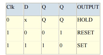
Truth Table for the D-type
Flip-flop
Frequency Division
One main
use of a Data Latch is as a Frequency Divider. In the Counters tutorials we saw
how the Data Latch can be used as a "Binary Divider", or a
"Frequency Divider" to produce a "divide-by-2" counter.
Here the inverted output terminal Q (NOT-Q) is connected directly back to the
Data input terminal D giving the device "feedback" as shown below.
Divide-by-2 Counter
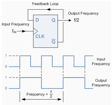
It can be
seen from the frequency waveforms above, that by "feeding back" the
output from Q to the input terminal D, the output pulses at Q have a frequency
that are exactly one half (f/2) that of the input clock frequency, (Fin).
In other words the circuit produces Frequency
Division as it now divides the input frequency by a factor of two (an
octave).
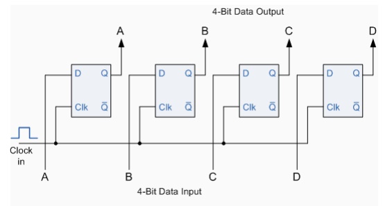
Another
use of a Data Latch is to hold or remember its data, thereby acting as a single
bit memory cell and IC's such as the TTL 74LS74 or the CMOS 4042 are available
in Quad format for this purpose. By connecting together four, 1-bit latches so that all their clock
terminals are connected at the same time a simple "4-bit" Data latch
can be made as shown below.
4-bit Data Latch
Transparent Data Latch
The Data Latch is a very useful devices in
electronic and computer circuits. They can be designed to have very high output
impedance at both outputs Q and its inverse Q to reduce the impedance effect on
the connecting circuit when used as buffers, I/O ports, bi-directional bus
drivers or even display drivers. But a single "1-bit" data latch is
not very practical to use on its own and instead commercially available IC's
incorporate 4, 8, 10, 16 or even 32 individual data latches into one single IC
package, and one such IC device is the 74LS373 Octal D-type transparent latch.
The eight
individual Data Latches of the 74LS373 are "transparent" D-type
latches, meaning that when the clock (CLK) input is HIGH at logic level
"1", the Q outputs follow the data D inputs and the latch appears
"transparent" as the data flows through it. When the clock signal is
LOW at logic level "0", the output is latched at the level of the
data that was present before the clock input changed.
8-bit Data Latch
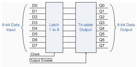
Functional
diagram of the 74LS373 Octal Transparent Latch
synchronous
(1)
Pertaining to two or more processes that depend upon the occurrence of
specific events such as common timing signals. (2) Occurring with a regular or
predictable time relationship.
counter (1) A
functional unit with a finite number of states each of which represents a
number that can be, upon receipt of an appropriate signal, increased by unity
or by a given constant. This device is usually capable of bringing the
represented number to a specified value; for example zero.
So a
"synchronous counter" is actually a functional unit with a certain
number of states, each representing a number which can be increaced or
decreased upon receiving an appropriate signal (e.g. a rising edge pulse), and
is usually used to count to, or count down to zero from, a specified number N.
.Basically,
any sequential circuit that goes through a prescribed sequence of
states upon the application of input pulses is called a counter. The input
pulses, called count pulses, may be clock pulses or they may originate from an
external source and may occur at prescribed intervals of time or at random. The
sequence of states in a counter may follow a binary count or any other
sequence.

Related Topics