Chapter: Electronic Circuits : JFET and MOSFET Amplifiers
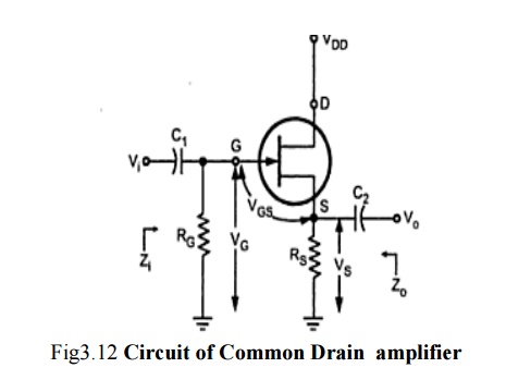
Common Drain Amplifier
In this circuit, input is applied between gate and source and output is taken between source and drain.
Common Drain Amplifier
In this
circuit, input is applied between gate and source and output is taken between
source and drain.
In this
circuit, the source voltage is
Vs
= VG+VGS
When a signal is applied to the JFET gate via C1 ,VG varies with the signal. As VGS is fairly constant and Vs = VG+VGS, Vs varies with Vi.
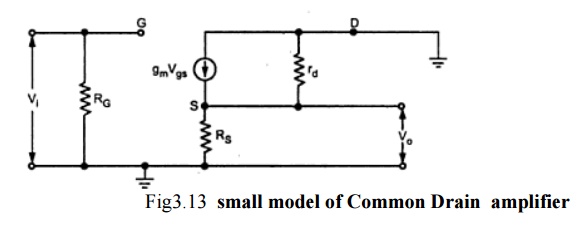
The
following figure shows the low frequency equivalent model for common drain
circuit.
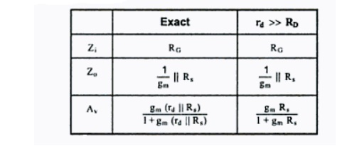
Input Impedance Zi
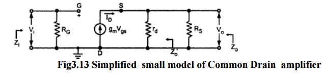
Zi = RG
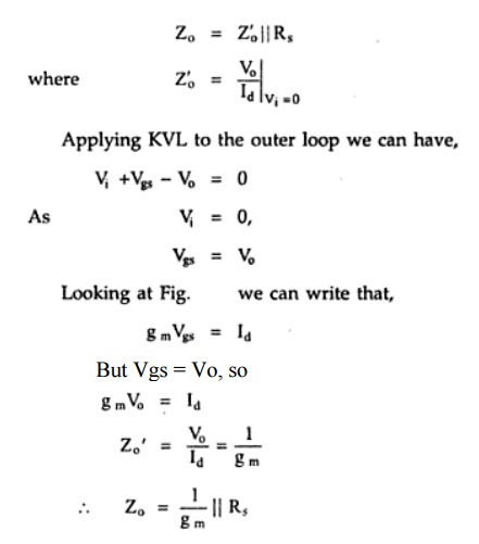
Output Impedance Zo
Voltage gain (Av)
It is given by
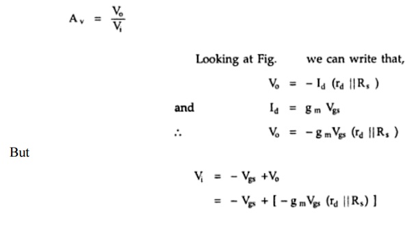
Substitute
the value Vo and Vi. Then
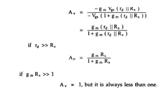
Common
drain circuit does not provide voltage gain.& there is no phase shift
between input and output voltages.
Table
summarizes the performance of common drain amplifier
Study Material, Lecturing Notes, Assignment, Reference, Wiki description explanation, brief detail
Electronic Circuits : JFET and MOSFET Amplifiers : Common Drain Amplifier |
Related Topics
Electronic Circuits : JFET and MOSFET Amplifiers