Applications of Operational Amplifier - Clipper and clipper using Operational Amplifier | Linear Integrated Circuits : Applications of Operational Amplifier
Chapter: Linear Integrated Circuits : Applications of Operational Amplifier
Clipper and clipper using Operational Amplifier
Clipper
and clipper
Applications:
Wave
shaping circuits are commonly used in digital computers and communication such
as TV and FM receiver.
Wave
shaping technique include clipping and clamping.
In
op-amp clipper circuits a rectifier diode may be used to clip off a certain
portion of the input signal to obtain a desired o/p waveform.
The
diode works as an ideal diode (switch) because when on, the voltage drop across
the diode is divided by the open loop gain of the op-amp. When off (reverse biased)
the diode is an open circuit. In an op-amp clamper circuits, however a
predetermined dc level is deliberately inserted in the o/p volt. For this
reason, the clamper is sometimes called a dc inverter.
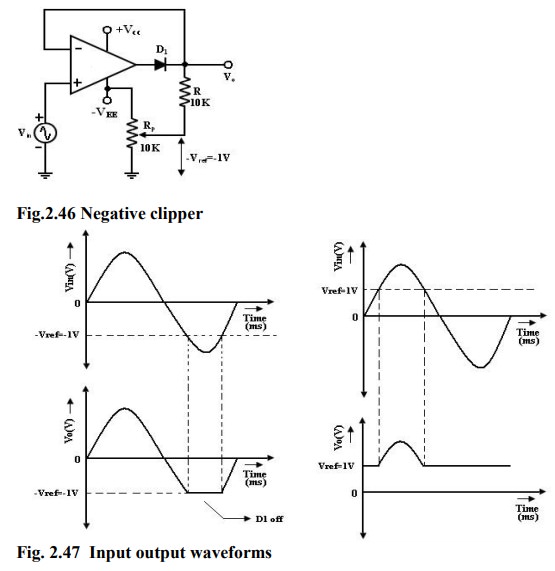
Positive
and Negative
Clipper: Positive Clipper:
A
circuit that removes positive parts of the input signal can be formed by using
an op-amp with a rectifier diode. T he clipping level is determined by the
reference voltage Vref, which should less than the i/p range of the
op-amp (Vref < Vin). The Output voltage has the
portions of the positive half cycles above Vref clipped off.
The
circuit works as follows:
During
the positive half cycle of the input, the diode D1 conducts only
until Vin = Vref. This happens because when Vin
<Vref, the output volts V0 of the op-amp becomes
negative to device D1 into conduction when D1 conducts it
closes feedback loop and op-amp operates as a voltage follower. (i.e.) Output
V0 follows input until Vin = Vref.
When
Vin > Vref => the V0 becomes +ve to
derive D1 into off. It opens the feedback loop and op- amp operates
open loop. When Vin drops below Vref (Vin<Vref)
the o/p of the op-amp V0 again becomes –ve to device D1
into conduction. It closes the feedback path. (o/p follows the i/p).
Thus
diode D1 is on for vin<Vref (o/p follows
the i/p) and D1 is off for Vin>Vref.
The
op-amp alternates between open loop (off) and closed loop operation as the D1
is turned off and on respectively. For this reason the op-amp used must be high
speed and preferably compensated for unity gain.
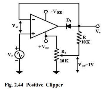
Ex: for high speed op-amp HA 2500, LM310, μA 318. In addition the difference input voltage (Vid=high) is high during the time when the feedback loop is open (D1 is off) hence an op-amp with a high difference input voltage is necessary to prevent input breakdown. If Rp (pot) is connected to –VEE instead of +Vcc, the ref voltage Vref will be negative (Vref = -ve). This will cause the entire o/p waveform above –Vref to be clipped off.
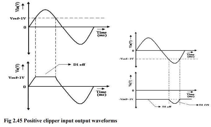
Negative Clipper:
The
positive clipper is converted into a –ve clipper by simply reversing diode D1
and changing the polarity of Vref voltage. The negative clipper
clips off the –ve parts of the input signal below the reference voltage. Diode
D1 conducts -> when Vin > -Vref and
therefore during this period o/p volt V0 follows the i/p volt Vin. The –Ve
portion of the output volt below –Vref is clipped off because (D1 is
off) Vin<-Vref. If –Vref is changed to –Vref
by connecting the potentiometer Rp to the +Vcc, the V0
below +Vref will be clipped off. The diode D1 must be on for Vin
> Vref and off for Vin.
Positive and Negative Clampers:
In
clamper circuits a predetermined dc level is added to the output voltage. (or)
The output is clamped to a desired dc level.
1. If the clamped dc level is +ve, the
clamper is positive clamper
2. If the clamped dc level is –ve, the
clamper is negative clamper.
Other
equivalent terms used for clamper are dc inserter or restorer. Inverting and
Non-Inverting that uses this technique.
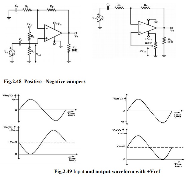
Capacitor:
The
Value of the capacitors in these circuits depends on different input rates and
pulse widths.
1.
In both circuits the dc level added to the o/p voltage is approximately equal
to Vcc/2.
2.
This +ve fixed dc level is needed to obtain a maximum undistorted symmetrical
sine wave.
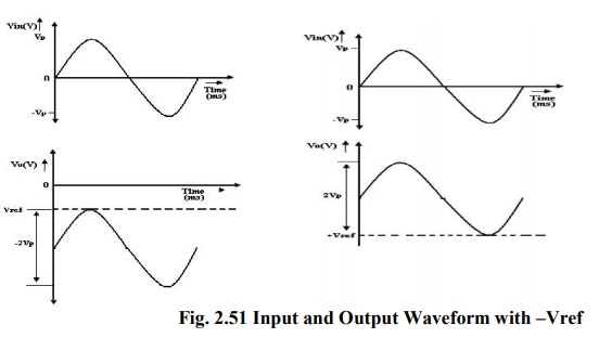
Peak clamper circuit:
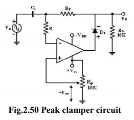
In
this circuit, the input waveform peak is clamped at Vref. For this reason, the
circuit is called the peak clamper.
First
consider the input voltage Vref at the (+) input: since this volt is +ve, V‘0
is also +ve which forward biases D1. This closed the feedback loop.
Voltage
Vin at the (-) input: During its –ve half cycle, diode D1
conducts, charging c; to the –ve peak value of Vp. During the +ve
half cycle, diode D1 in reverse biased. Since this voltage Vp is in series with
the +ve peak volt Vp the o/p volt V0 = 2 Vp. Thus the nett o/p is Vref plus 2
Vp. So the – ve peak of 2 Vp is at Vref. For precision clamping, CiRd
<< T/2
Where
Rd = resistance of diode D1 when it is forward biased.
T
= time period of the input waveform.
Resistor
R is used to protect the op-amp against excessive discharge currents from
capacitor Ci especially when the dc supply voltages are switched off. A +ve
peak clamping is accomplished by reversing D1 and using –ve reference voltage
(-Vref).
Note:
Inv
and Non-Inv clamper – Fixed dc level
Peak
clamper – Variable dc level
Related Topics