Chapter: Digital Principles and System Design : Combinational logic
Circuits for Arithmetic operations
CIRCUITS FOR ARITHMETIC
OPERATIONS
Arithmetic circuits are the ones
which perform arithmetic operations like addition, subtraction, multiplication,
division, parity calculation. Most of the time, designing these circuits is the
same as designing mux, encoders and decoders.
1.
Adders
Adders are the basic building
blocks of all arithmetic circuits; adders add two binary numbers and give out
sum and carry as output. Basically we have two types of adders.
· Half Adder.
·
Full Adder.
ü
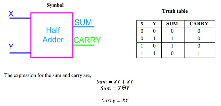
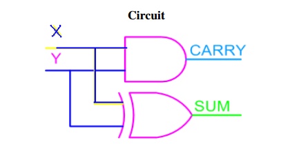
Half Adder
A half-adder is an arithmetic
circuit block that can be used to add two bits. Such a circuit thus has two
inputs that represent the two bits to be added and two outputs, with one
producing the SUM output and the other producing the CARRY.
Adding two single-bit binary values X, Y produces
a sum S bit and a carry out C-out bit. This operation is called half addition
and thus the circuit to realize it is called a half adder.
ü
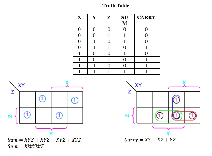
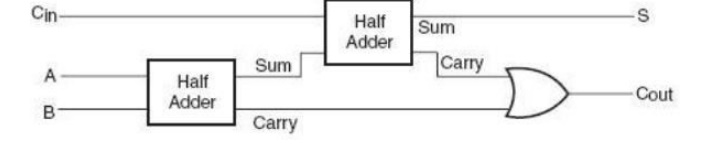
Full Adder
A full adder circuit is an
arithmetic circuit block that can be used to add three bits to produce a SUM
and a CARRY output. Such a building block becomes a necessity when it comes to
adding binary numbers with a large number of bits. The full adder circuit
overcomes the limitation of the half-adder, which can be used to add two bits
only.
Full adder takes a three-bits input. Adding two single-bit
binary values X, Y with a carry input bit C-in produces a sum bit S and a carry
out C.
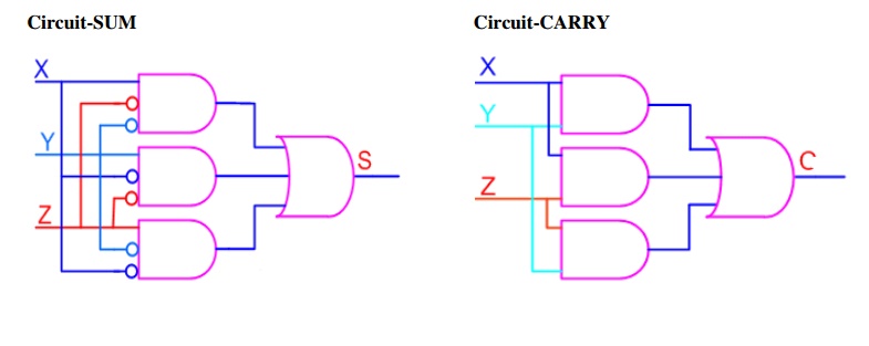
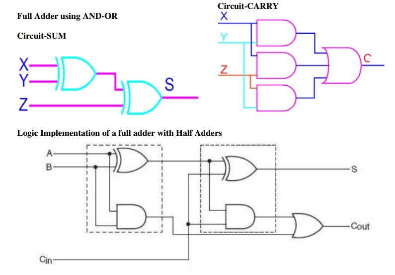
Full Adder using AND-OR
The below implementation shows
implementing the full adder with AND-OR gates, instead of using XOR gates. The
basis of the circuit below is from the above K-map
Circuit-SUM Circuit-CARRY
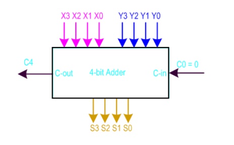
ü n-bit Carry Ripple Adder
An n-bit adder used to add two
n-bit binary numbers can be built by connecting n full adders in series. Each
full adder represents a bit position j (from 0 to n-1).
Each carry out C-out from a full
adder at position j is connected to the carry in C-in of the full adder at
higher position j+1. The output of a full adder at position j is given by:
Sj= Xj Yj Cj
Cj+1 = Xj
. Yj + Xj . Cj + Y . Cj
In the expression of the sum Cj
must be generated by the full adder at lower position j. The propagation delay
in each full adder to produce the carry is equal to two gate delays = 2 D Since
the generation of the sum requires the propagation of the carry from the lowest
position to the highest position , the total propagation delay of the adder is
approximately:
Total Propagation delay = 2 nD
4-bit Carry Ripple Adder
Adds two 4-bit numbers:
X = X3 X2 X1 X0
Y = Y3 Y2 Y1 Y0
Producing the sum S = S3 S2 S1 S0, C-out = C4 from
the most significant position j=3 Total Propagation delay = 2 nD = 8D or 8 gate
delays
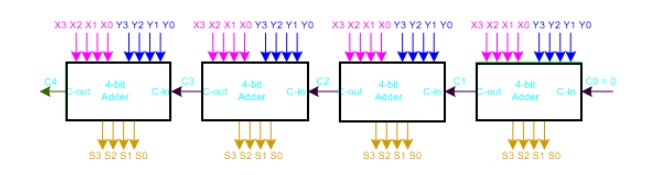
Larger Adder
Example: 16-bit adder using 4
4-bit adders. Adds two 16-bit inputs X (bits X0 to X15), Y (bits Y0 to Y15)
producing a 16-bit Sum S (bits S0 to S15) and a carry out C16 from the most
significant position. Propagation delay for 16-bit adder = 4 x propagation
delay of 4-bit adder
= 4 x 2 nD = 4 x 8D = 32 D or 32 gate delays
ü
Carry Look-Ahead Adder
The delay generated by an N-bit
adder is proportional to the length N of the two numbers X and Y that are added
because the carry signals have to propagate from one full-adder to the next.
For large values of N, the delay becomes unacceptably large so that a special
solution needs to be adopted to accelerate the calculation of the carry bits.
This solution involves a "look-ahead carry generator" which is a
block that simultaneously calculates all the carry bits involved. Once these bits
are available to the rest of the circuit, each individual three-bit addition (Xi+Yi+carry-ini)
is implemented by a simple 3-input XOR gate. The design of the look-ahead carry
generator involves two Boolean functions named Generate and Propagate. For each
input bits pair these functions are defined as: Gi = Xi . Yi & Pi = Xi + Yi
The carry bit c-out(i) generated
when adding two bits Xi and Yi is '1' if the corresponding function Gi is '1'
or if the c-out(i-1)='1' and the function Pi = '1' simultaneously. In the first
case, the carry bit is activated by the local conditions (the values of Xi and
Yi). In the second, the carry bit is received from the less significant
elementary addition and is propagated further to the more significant
elementary addition. Therefore, the carry_out bit corresponding to a pair of
bits Xi and Yi is calculated according to the equation:
carry_out(i) = Gi + Pi.carry_in(i-1)
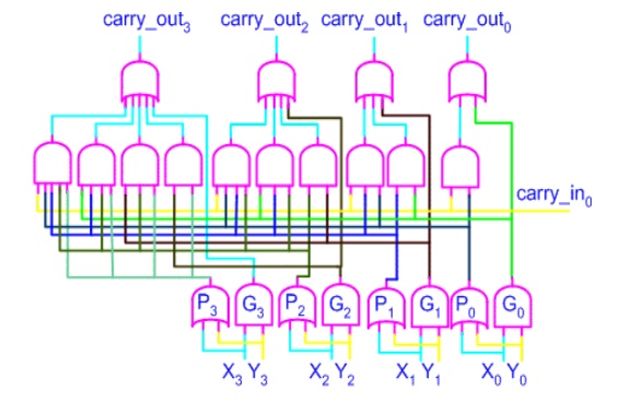
For a four-bit adder the carry-outs are calculated as follows
carry_out0 = G0 + P0 . carry_in0
carry_out1 = G1 + P1 . carry_out0
= G1 + P1G0 + P1P0 . carry_in0 carry_out2 = G2 + P2G1 + P2P1G0 + P2P1P0 .
carry_in0
carry_out3 = G3 + P3G2 + P3P2G1 + P3P2P1G0 + P3P2P1 .
carry_in0
The set of equations above are
implemented by the circuit below and a complete adder with a look-ahead carry
generator is next. The input signals need to propagate through a maximum of 4
logic gate in such an adder as opposed to 8 and 12 logic gates in its
counterparts illustrated earlier.
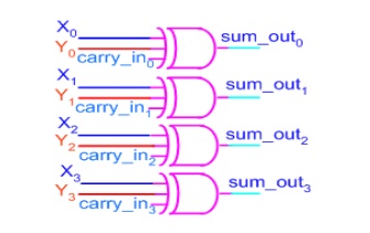
Sums can be calculated from the
following equations, where carry_out is taken from the carry calculated in the
above circuit.
sum_out0 = X 0 Y0 carry_out0 sum_out1 = X 1 Y1
carry_out1 sum_out2 = X 2 Y2 carry_out2 sum_out3 = X 3 Y3 carry_out3
ü
BCD Adder
BCD addition is the same as
binary addition with a bit of variation: whenever a sum is greater than 1001,
it is not a valid BCD number, so we add 0110 to it, to do the correction. This
will produce a carry, which is added to the next BCD position.
·
Add the two 4-bit BCD code inputs.
·
Determine if the sum of this addition is greater than 1001; if yes, then add
0110 to this sum and generate a carry to the next decimal position
2. Subtractor
Subtractor circuits take two binary numbers as input and
subtract one binary number input from the other
binary number input. Similar to adders, it gives out two
outputs, difference and borrow (carry-in the case
of Adder). The
BORROW output here specifies whether a ‗1‘ has been borrowed to theperform
subtraction.
There are two types of subtractors,
ü
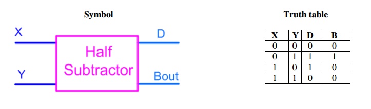
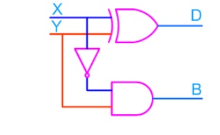
Half Subtractor
The half-subtractor is a
combinational circuit which is used to perform subtraction of two bits. It has
two inputs, X (minuend) and Y (subtrahend) and two outputs D (difference) and B
(borrow). The logic symbol and truth table are shown below.
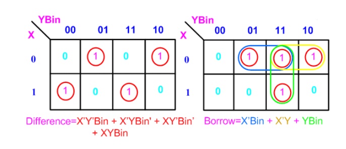
From the above table we can draw the K-map as
shown below for "difference" and "borrow". The Boolean
expression for the difference and Borrow can be written.
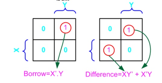
From the equation we can draw the half-subtractor
as shown in the figure below.
ü Full Subtractor
A full subtractor
is a combinational
circuit that performs
subtraction involving three
bits, namely
minuend, subtrahend, and
borrow-in. There are two outputs, namely the DIFFERENCE output D and the BORROW
output Bo. The BORROW output bit tells whether the
minuend bit needs to borrow a
from the next possible higher minuend bit. The logic symbol
and truth table are shown below.
Symbol
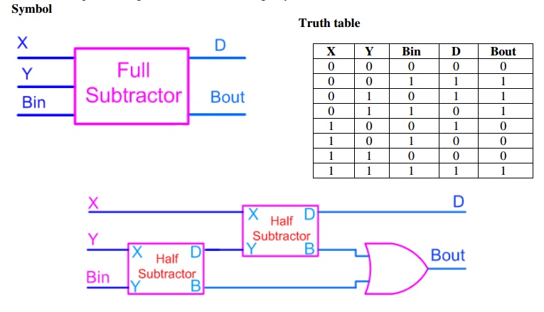
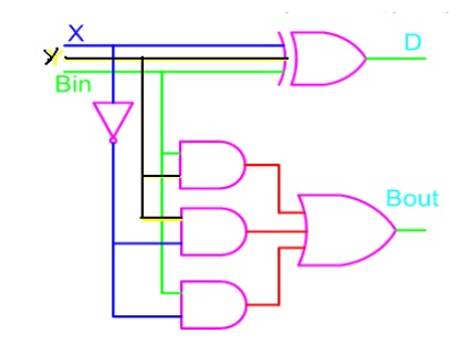
From the above expression, we can draw the circuit
below. If you look carefully, you will see that a full-subtractor circuit is
more or less same as a full-adder with slight modification.
ü
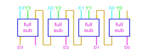
Parallel Binary Subtractor
Parallel binary subtractor can be
implemented by cascading several full-subtractors. Implementation and associated
problems are those of a parallel binary adder, seen before in parallel binary
adder section.
Below is the block level representation of a 4-bit
parallel binary subtractor, which subtracts 4-bit Y3Y2Y1Y0 from 4-bit X3X2X1X0.
It has 4-bit difference output D3D2D1D0 with borrow output Bout.
ü
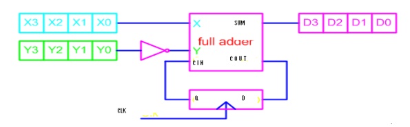
Serial Binary Subtracter
A serial subtracter can be obtained by converting
the serial adder using the 2's complement system. The subtrahend is stored in
the Y register and must be 2's complemented before it is added to the minuend
stored in the X register. The circuit for a 4-bit serial subtracter using
full-adder is shown in the figure below.
ü
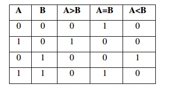
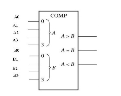
Comparators
It is a combinational
circuit that compares two numbers and determine their
relative magnitude. The output of comparator is usually 3 binary variables
indicating:
A<B,
A=B, A>B
1-bit comparator: Let’sbegin
with 1 bit comparator and from the name we can easily make out that this
circuit would be used to compare 1 bit binary numbers.
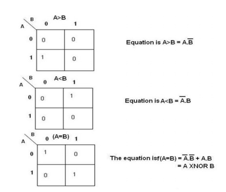
For a 2-bit comparator we have four inputs A1A0
and B1B0 and three output E ( is 1 if two numbers are equal) G (is 1 when A
> B) and L (is 1 when A < B) If we use truth table and K-map the result
is
The comparison process of two
positive numbers X and Y is performed in a bit-by-bit manner starting with the
most significant bit:
If the
most significant bits are Xn='1' and Yn='0' then number X is larger than Y.
·
If Xn='0' and Yn='1' then number X is smaller than
Y.
·
If Xn=Yn then no decision can be taken about X and
Y based only on these two bits.
If the most significant bits are
equal then the result of the comparison is determined by the less significant
bits Xn-1 and Yn-1. If these bits are equal as well, the process continues with
the next pair of bits. If all bits are equal then the two numbers are equal.
4-bit comparator:
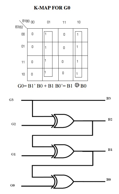
CODE CONVERSION-
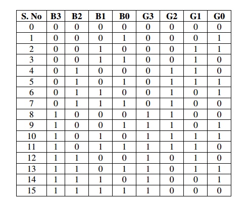
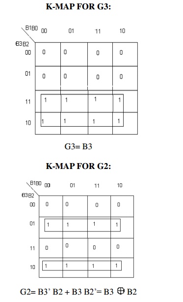
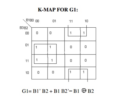
Binary to Gray converter
Truth Table
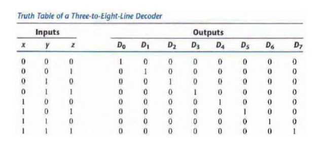
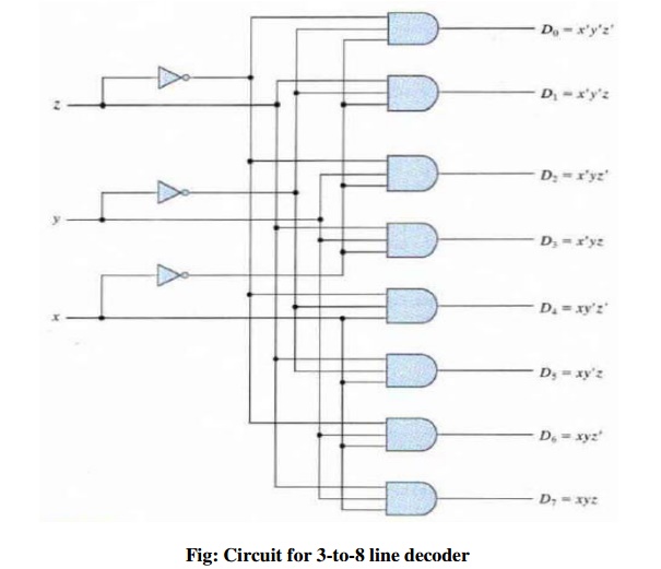
DECODERS
A decoder circuit can be used to implement AND-OR circuit
SOP Boolean expression when decoder active state output is 1 and inactive 0 .
•
Number of binary inputs = n
•
Number of binary outputs = 2n = Maximumumber n
of
minterms, where n is the number of literals in F
• Its outputs reflect the-Mini terms with one term each at each of the output
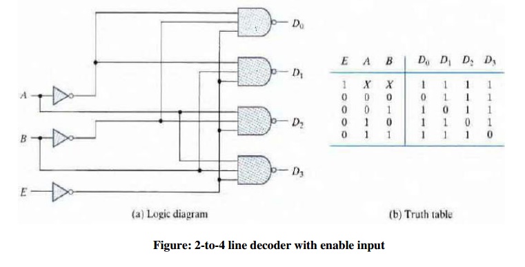
ENCODERS
An encoder is a circuit
that converts the binary information from one form to another. Gives a unique
combination of outputs according to the information at a unique input at
one-line (or at multiple lines).
Action of a one active line input
encoder is opposite of that of a one active line output decoder. An encoder,
which has multi-lines as the active inputs, is also
called ‘priority encoder’. Encoder
differentiated from decoder by
greater number of inputs than outputs compared to the decoder. The priority
encoder includes a priority function.
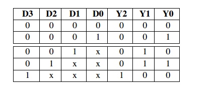
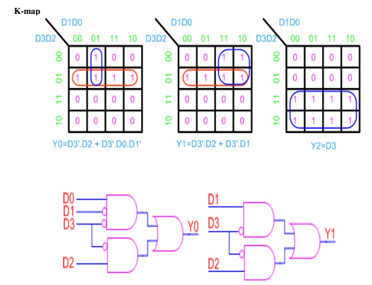
4to3 Priority Encoder-The truth
table of a 4-input priority encoder is as shown below. The input D3 has the
highest priority, D2 has next highest priority, D0 has the lowest priority.
This means output Y2 and Y1 are 0 only when none of the inputs D1, D2, D3 are
high and only D0 is high. A 4 to 3 encoder consists of four inputs and three
outputs, truth table and symbols of which is shown below.
Truth Table
MULTIPLEXERS
Many tasks in communications, control, and
computer systems can be performed by combinational logic circuits. When a
circuit has been designed to perform some task in one application, it often
finds use in a different application as well.
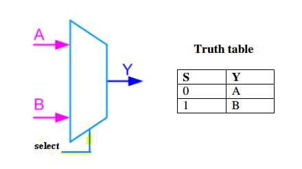
A multiplexer (MUX) is a digital switch
which connects data from one of n sources to the output. A number of select
inputs determine which data source is connected to the output. The block
diagram of MUX with n data sources of b bits wide and s bits wide select line
is shown in below figure.

Example - 2x1 MUX
A 2 to 1 line multiplexer is shown in figure
below, each 2 input lines A to B is applied to one input of an AND gate. Selection
lines S are decoded to select a particular AND gate. The truth table for the
2:1 mux is given in the table below.
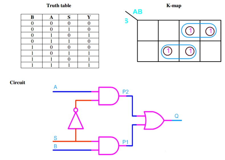
Design of a 2:1 Mux
To derive the gate level
implementation of 2:1 mux we need to have truth table as shown in figure. And
once we have the truth table, we can draw the K-map as shown in figure for all
the cases when Y is equal to '1'.
Combining
the two 1' as shown in figure, we can drive the output y as shown below
Y = A.S'
+ B.S
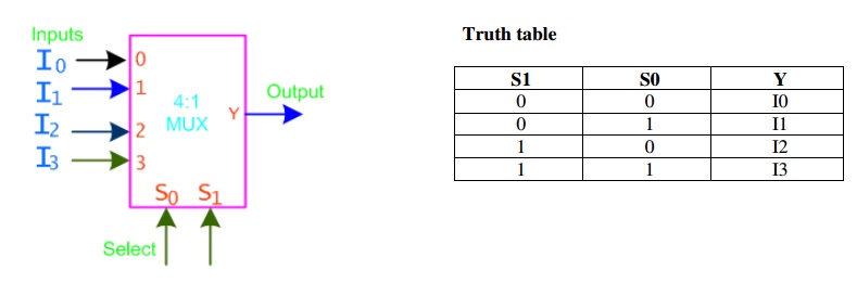
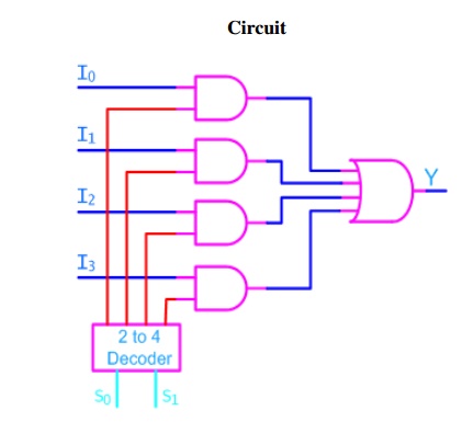
Example : 4:1 MUX
A 4 to 1 line multiplexer is shown in figure
below, each of 4 input lines I0 to I3 is applied to one input of an AND gate.
Selection lines S0 and S1 are decoded to select a particular AND gate. The
truth table for the 4:1 mux is given in the table below.
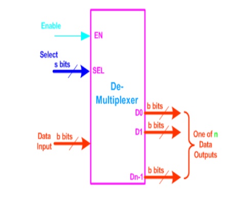
DEMULTIPLEXERS
They are digital switches which
connect data from one input source to one of n outputs. Usually implemented by
using n-to-2n binary decoders where the decoder enable line is used for data
input of the de-multiplexer.
The figure below shows a
de-multiplexer block diagram which has got s-bits-wide select input, one
b-bits-wide data input and n b-bits-wide outputs.
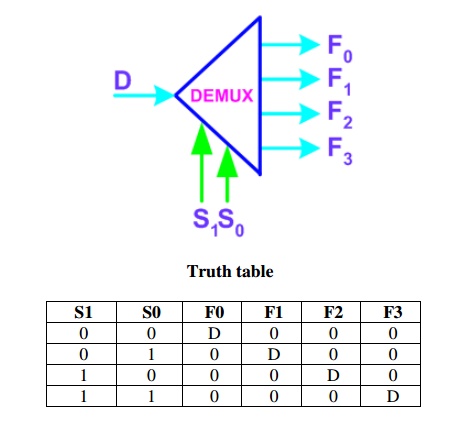
Example: 1-to-4 De-multiplexer
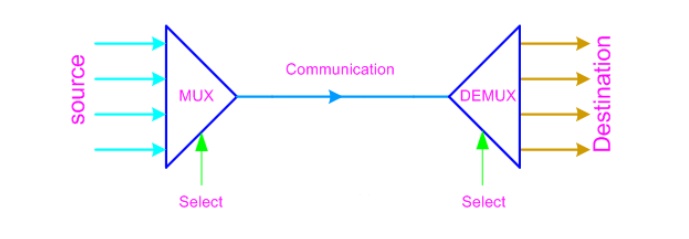
Mux- Demux: Application Example
This enables sharing a single communication line
among a number of devices. At any time, only one source and one destination can
use the communication line.
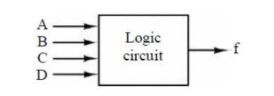
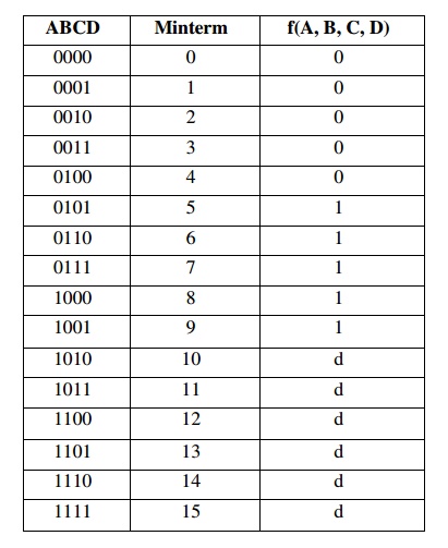
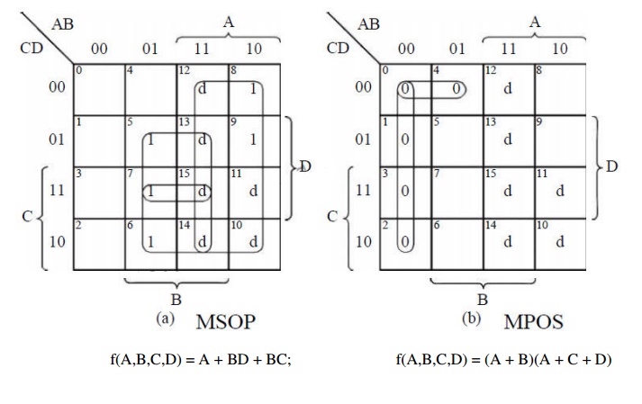
Example: Design a circuit
to distinguish BCD digits ≥ 5 from those < 5.
Related Topics