Chapter: VLSI Design : Combinational and Sequential Circuit Design
Circuit Design of Latches and Flip Flops
CIRCUIT DESIGN OF LATCHES AND
FLIP FLOPS:
Another
class of logic circuits are sequential circuits. These circuits are two-valued
networks in which the outputs at any instant are dependent not only upon the
inputs present at that instant but also upon the past history (sequence) of
inputs.
Sequential
circuits are classified into:
§ Synchronous sequential circuits –Their
behaviour is determined by the values of thesignals at only discrete instants
of time.
§ Asynchronous
sequential circuits –Their behaviour
is immediately affected by the input signal changes.
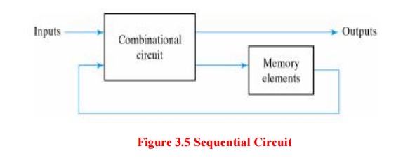
The block
diagram of a sequential circuit is shown below:
The basic
logic element that provides memory in many sequential circuits is the
flip-flop.
1. Latches
Latches
form one class of flip-flops. This class is characterized by the fact that the
timing of the output changes is not controlled. Although latches are useful for
storing binary information and for the design of asynchronous sequential
circuits, they are not practical for use in synchronous sequential circuits.
2. The SR Latch
It is a
circuit with two cross-coupled NOR gates or two cross-coupled NAND gates. The
one with NOR gates is shown below:
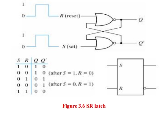
The
condition that is undefined is when both inputs are equal to 0 at the same
time. Comparing the NAND with the NOR latch note that the input signals for the
NAND require the complement of those values used for the NOR latch.
Because
the NAND latch requires a 0 signal to change its state, it is sometimes
referred to as an S′-R′ latch. The operation of the SR latch can be modified to
provide an additional control input that determines when the state of the latch
can be changed.
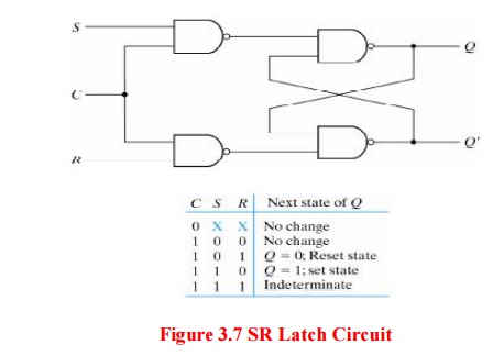
An SR
latch with control input is shown below: The control input C acts as an enable
signal form the other two inputs.
An indeterminate
condition occurs when all three inputs are equal to 1. This condition makes the
circuit difficult to manage and is seldom used in practice.
Nevertheless,
it is an important circuit because other latches and flip-flops are realized
from it.
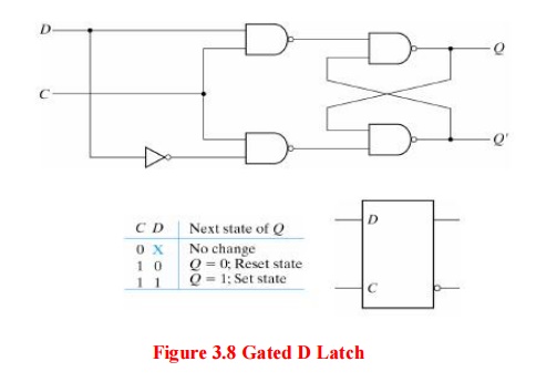
3. The Gated D Latch
One way
to eliminate the undesirable condition of the indeterminate state in the SR
latch is to ensure that inputs S and R are never equal to 1 at the same time.
This is done by the D latch
4. Flip-Flops
When
latches are used for the memory elements in sequential circuits, a serious
difficulty arises. Recall that latches have the property of immediate output
responses (i.e., transparency).
Because
of this the output of a latch cannot be applied directly (or through logic) to
the input of the same or another latch when all the latches are triggered by a
common clock source. Flip -flops are used to overcome this difficulty.
5. Edge-Triggered D
Flip-Flop
A D
flip-flop may be realized with two D latches connected in a master-slave
configuration: The circuit samples the D input and changes its Q output only at
the negative-edge of the controlling clock signal (CLK).
It is
also possible to design the circuit so that the flip-flop output changes on the
positive edge of the clock (transition from 0 to 1).
This
happens in a flipflop that has an additional inverter between the CLK terminal
and the junction between the other inverter and input C on the master latch. An
efficient realization of a positive edge-triggered D flip-flop uses three SR
latches:
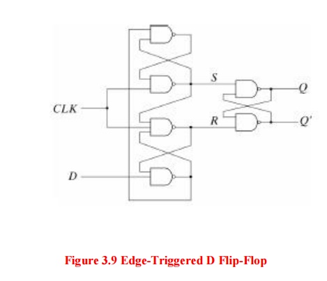
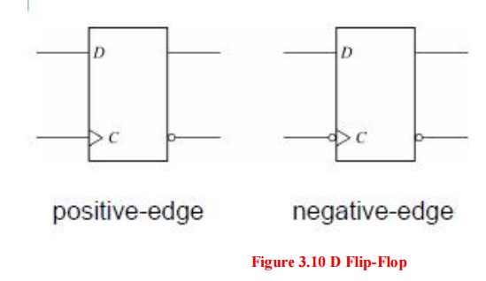
The graphic symbol for the edge-triggered D flipflop is:
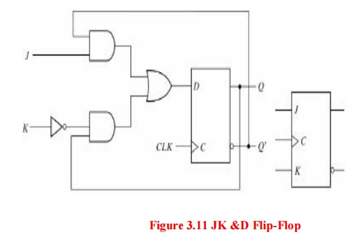
6. Other Flip-Flops
The most
economical and efficient flip-flop in terms of transistor count and silicon
area is the D flip-flop. Other types of flip-flops can be realized by using the
D flip-flop and external logic.
Two
flipflops widely used in the design of digital systems are the JK and the T
flip-flops. There are three operations that can be performed with a flip-flop:
set it to 1, reset it to 0, complement its output. The JK flip-flop performs
all three:
7. Characteristic
Tables
A
characteristic table defines the logical properties of a flip-flop by
describing its operation in tabular form. The flip-flops characteristic tables
are:
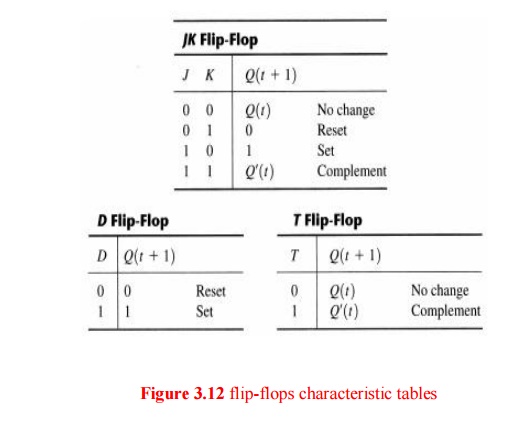
Q(t)
refers to the present state prior to the application of a clock edge.
Q(t + 1)
is the next state one clock period later. The clock edge input is not included
in the characteristic tables, but is implied to occur between time t and t + 1.
8. Characteristic
Equations
The
logical properties of a flip-flop as described in its characteristic table can
be expressed also algebraically with a characteristic equation. For the D
flip-flop the characteristic equation is:
Q(t +1) =
D
It states
that the next state of the output will be equal to the value of input D in the
present state.
The
characteristic equation for the JK flip-flop is:
Q(t+1)=JQ’+K’Q
where Q
is the value of the flip-flop output prior to the application of a clock edge.
Finally, the characteristic equation for the T flipflop is:
Q(t+1)=TQ’+T’Q
Related Topics