Chapter: Linear Integrated Ciruits : Spical ICs
Block Diagram of 555 Timer IC
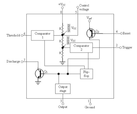
Block Diagram of 555 Timer IC:

From the
above figure, three 5k internal resistors act as voltage divider providing bias
voltage of 2/3 Vcc to the upper comparator & 1/3 Vcc to the lower
comparator. It is possible to vary time electronically by applying a modulation
voltage to the control voltage input terminal (5).
(i) In the
Stable state:
The
output of the control FF is high. This means that the output is low because of
power amplifier which is basically an inverter. Q = 1; Output = 0
(ii) At the
Negative going trigger pulse:
The
trigger passes through (Vcc/3) the output of the lower comparator goes high
& sets the
FF.Q = 1;
Q = 0
(iii) At the
Positive going trigger pulse: It passes through 2/3Vcc, the output of the upper
comparator goes high and resets the FF. Q = 0; Q = 1 The reset input (pin 4)
provides a mechanism to reset the FF in a manner which overrides the effect of
any instruction coming to FF from lower comparator.
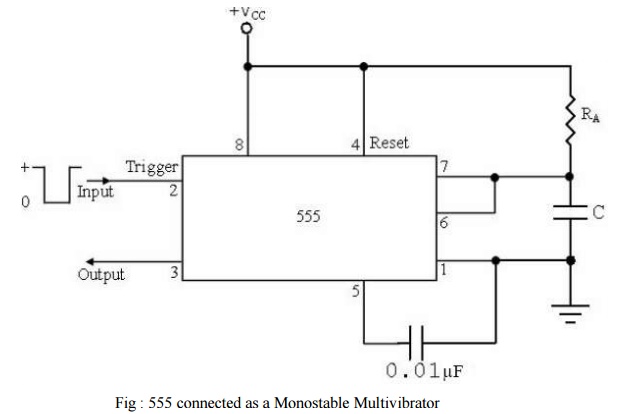
Monostable Operation:
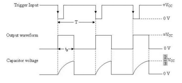
Model Graph:
Initially
when the output is low, i.e. the circuit is in a stable state, transistor Q1
is ON & capacitor C is shorted to ground. The output remains low. During
negative going trigger pulse, transistor Q1 is OFF, which releases
the short circuit across the external capacitor C & drives the output high.
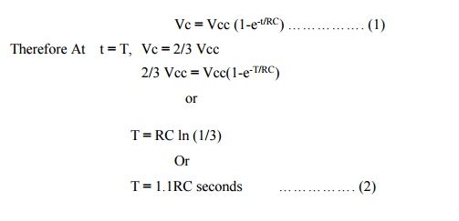
Now the capacitor C starts charging toward Vcc through RA. When the voltage
across the capacitor equals 2/3 Vcc, upper comparator switches from
low to high. i.e. Q = 0, the transistor Q1 = OFF ; the output is
high.
Since C
is unclamped, voltage across it rises exponentially through R towards Vcc
with a time constant RC (fig b) as shown in below. After the time period, the upper
comparator resets the FF, i.e. Q = 1, Q1 = ON; the output is
low.[i.e discharging the capacitor C to ground potential (fig c)]. The voltage
across the capacitor as in fig (b) is given by
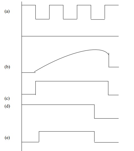
If the
reset is applied Q2 = OFF, Q1 = ON, timing capacitor C
immediately discharged. The output now will be as in figure (d & e). If the
reset is released output will still remain low until a negative going trigger
pulse is again applied at pin 2.
Related Topics