Chapter: Electronic Circuits : Biasing of Discrete BJT and MOSFET
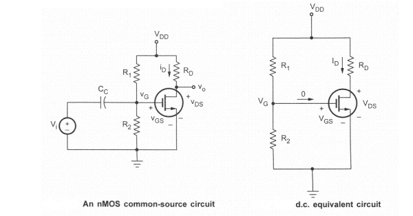
Biasing of MOSFET
Biasing of MOSFET
*N-channel
enhancement mode MOSFET circuit shows the source terminal at ground potential
and is common to both the input and output sides of the circuit. *The coupling
capacitor acts as an open circuit to d.c. but it allows the signal voltage to
be coupled to the gate of the MOSFET
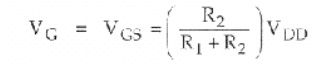
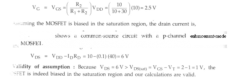
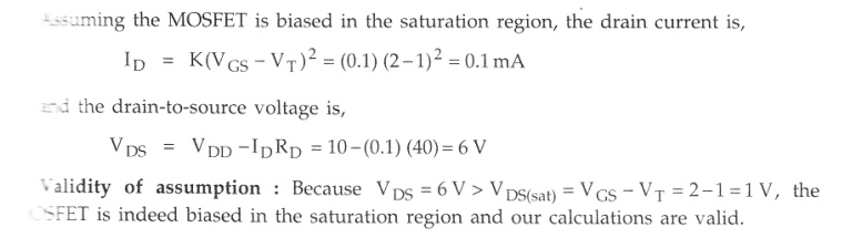
Assume VG > VT , MOSFET is biased in the saturation region, the drain current is,
Biased in
the nonsaturation region, and the drain current is given by, ID
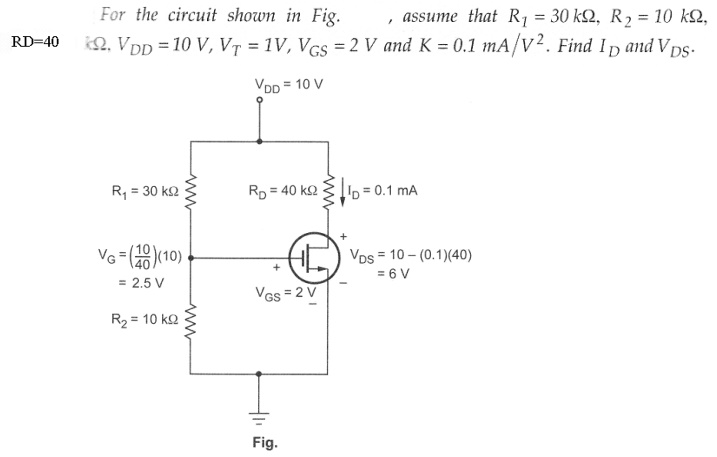
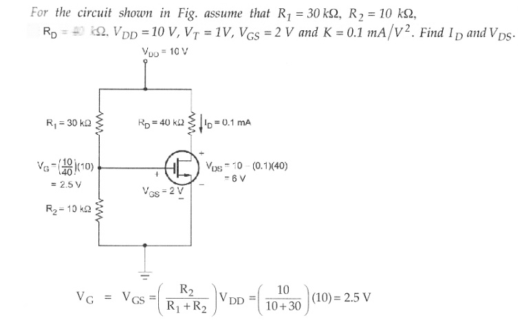
Example problem-1
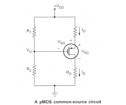
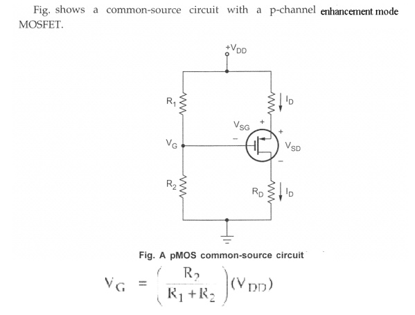
Here, the source is tied to +VDD, Which become signal ground in the a.c. equivalent circuit. Thus it is also a common-source circuit.
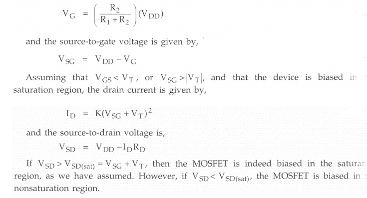
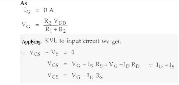
The d.c. analysis for this circuit is essentially the same as for the n-channel MOSFET circuit. The gate voltage is given by,
Load Line and Modes of Operation
The load
line gives a graphical picture showing the region in whichthe MOSFET is biased.
Consider the common-source circuit shown in Fig. (a).
Writing
Kirchhoff's voltage law around the drain-source loop results VDs = VDD
-IDRD, which is the load line equation. It shows a linear
relationship between the drain current and drain-to-source voltage. Fig. (b)
shows the VDS(sat) characteristic for the MOSFET
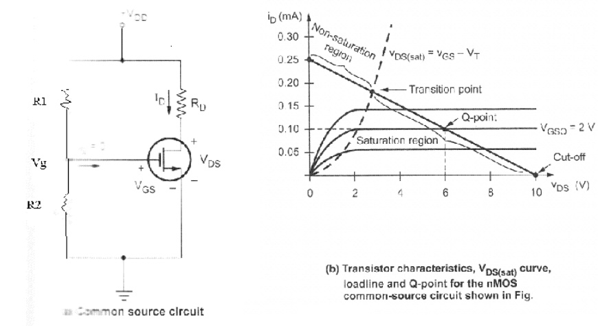
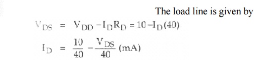
The two
end points of the load line are determine in the usual manner. If the drain
current = 0, then VDS= 10 v; if VDS = 0, then drain
current = 10/40 = 0.25 mA. The Q-point of the MOSFET is given by the d.c. drain
current (ID) and drain-to-source voltage (VDS) and it is
always on the load line, as shown in the Fig. b).
If the
gate-to-source voltage is less than V1, the drain current is zero and the
MOSFET is in cut-off. As the gate-to- source voltage becomes just greater than
the threshold voltage, the MOSFET turns ON and is biased in the saturation
region. As V GS increases, the Q-point moves up the load line. The
transition point is the boundary between the saturation and non-saturation
regions. It is the point where,

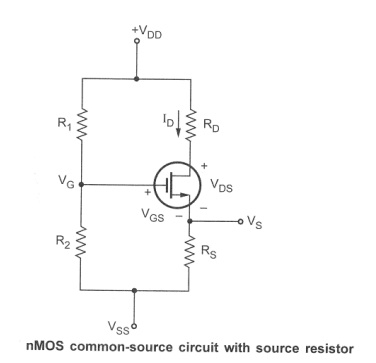
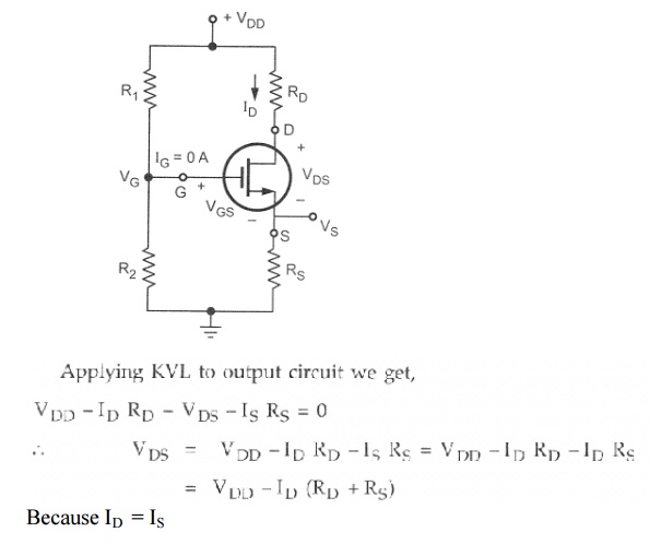
Common Source circuit for EMOSFET with source
resistor
Voltage Divider Bias
Biasing Circuit for D MOSFET
Biasing
circuits for depletion type MOSFET are quite similar to the circuits used for
JFET biasing. The primary difference between the two is the fact that depletion
type MOSFETs also permit operating points with positive value of V6s for
n-channel and negative values of V6s for p-channel MOSFET. To have positive
value of V GS for n-channel and negative value of V6s for p-channel
self bias circuit is unsuitable.
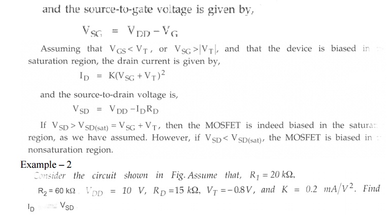
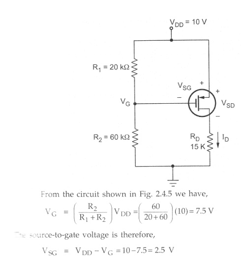
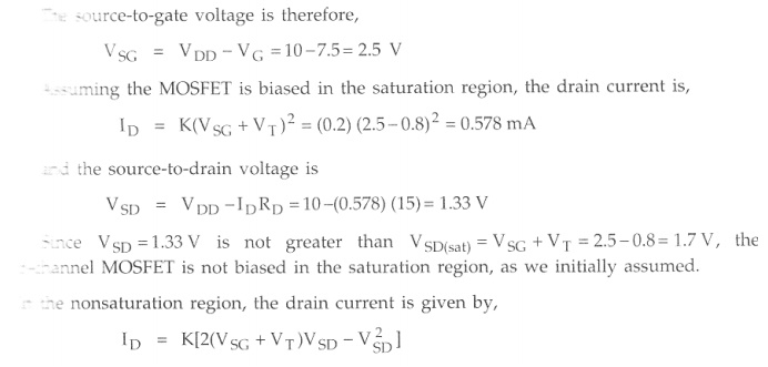
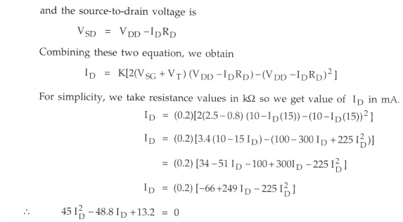
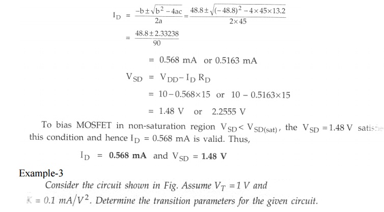
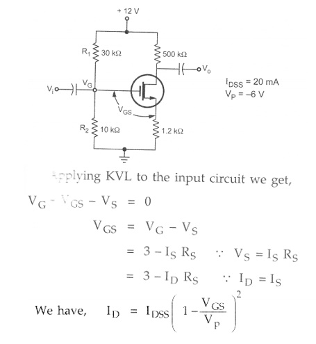
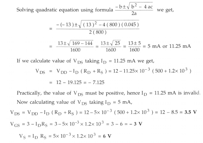
Example
problem-1
Related Topics