Chapter: Electronic Devices and Circuits : Transistors
Biasing: Fixed Bias or Base Bias and Stability of Operating Point
BIASING
Fixed Bias or Base Bias:
In order for a transistor to amplify, it has to be properly biased. This means forward biasing the base emitter junction and reverse biasing collector base junction. For linear amplification, the transistor should operate in active region ( If IE increases, IC increases, VCE decreases proportionally).
The source VBB, through a current limit resistor RB forward biases the emitter diode and VCC through resistor RC (load resistance) reverse biases the
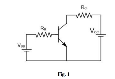
The dc base current through RB is given by
IB = (VBB - VBE) / RB
or VBE = VBB - IB RB
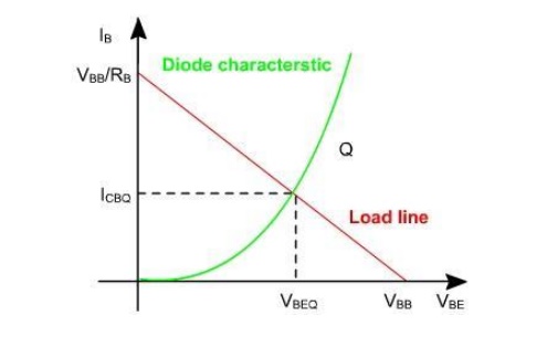
Normally VBE is taken 0.7V or 0.3V. If exact voltage is required, then the input characteristic ( IB vs V BE) of the transistor should be used to solve the above equation. The load line for the input circuit is drawn on input characteristic. The two points of the load line can be obtained as given below
For IB = 0, VBE = VBB.
and For VBE = 0, IB = VBB/ RB.
The intersection of this line with input characteristic gives the operating point Q as shown in fig. 2. If an ac signal is connected to the base of the transistor, then variation in VBE is about Q point. This gives variation in IB and hence IC.
In the output circuit, the load equation can be written as
VCE = VCC- IC RC
This equation involves two unknown VCE and IC and therefore can not be solved. To solve this equation output characteristic ( ICvs VCE) is used.
The load equation is the equation of a straight line and given by two points: IC= 0,
VCE = VCC
& VCE = 0,IC= VCC / RC
The intersection of this line which is also called dc load line and the characteristic gives the operating point Q as shown in fig. 3.
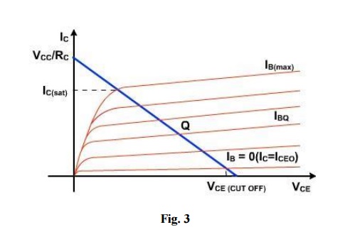
The point at which the load line intersects with IB = 0 characteristic is known as cut off point. At this point base current is zero and collector current is almost negligibly small. At cut off the emitter diode comes out of forward bias and normal transistor action is lost. To a close approximation.
VCE ( cut off)VCC (approximately).
The intersection of the load line and IB = IB(max) characteristic is known as saturation point
. At this point IB= IB(max), IC= IC(sat). At this point collector diodes comes out of reverse bias and again transistor action is lost. To a close approximation,
IC(sat) VCC / RC(approximately ).
The IB(sat) is the minimum current required to operate the transistor in saturation region. If the IB is less than IB (sat), the transistor will operate in active region. If IB > IB(sat) it always operates in saturation region.
If the transistor operates at saturation or cut off points and no where else then it is operating as a switch is shown in fig. 4.
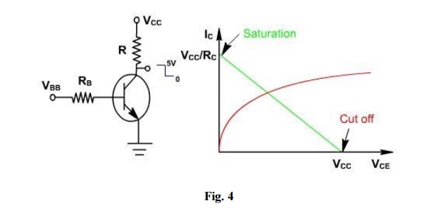
VBB = IB RB+ VBE
IB = (VBB – VBE ) / RB
If IB> IB(sat), then it operates at saturation, If IB = 0, then it operates at cut off.
If a transistor is operating as an amplifier then Q point must be selected carefully. Although we can select the operating point any where in the active region by choosing different values of RB & RC but the various transistor ratings such as maximum collector dissipation PC(max) maximum collector voltage VC(max) and IC(max) & VBE(max) limit the operating range.
Once the Q point is established an ac input is connected. Due to this the ac source the base current varies. As a result of this collector current and collector voltage also varies and the amplified output is obtained.
If the Q-point is not selected properly then the output waveform will not be exactly the input waveform. i.e. It may be clipped from one side or both sides or it may be distorted one.
Ø Stability of Operating Point
Let us consider three operating points of transistor operating in common emitter amplifier.
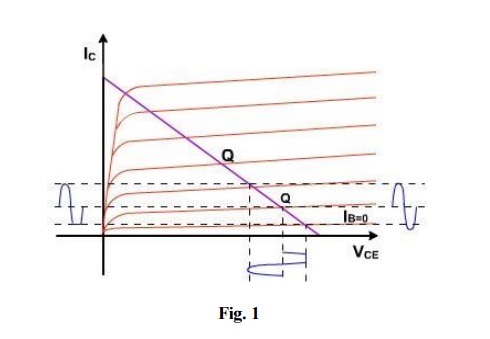
1. Near cut off
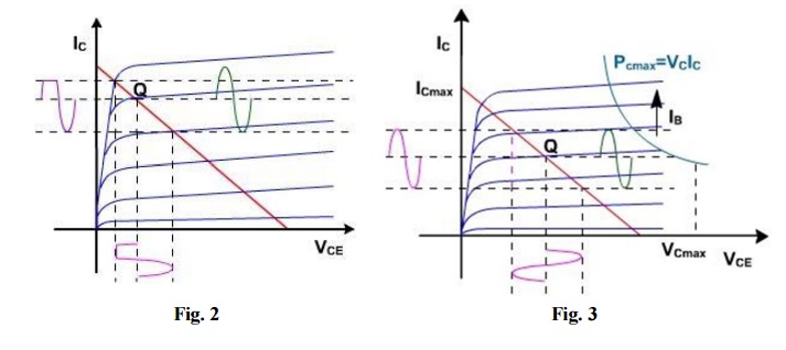
. Near saturation
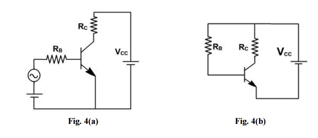
3. In the middle of active region
If the operating point is selected near the cutoff region, the output is clipped in negative half cycle as shown in fig. 1.
If the operating point is selected near saturation region, then the output is clipped in positive cycle as shown in fig. 2.
If the operating point is selected in the middle of active region, then there is no clipping and the output follows input faithfully as shown in fig. 3. If input is large then clipping at both sides will take place. The first circuit for biasing the transistor is CE configuration is fixed bias.
In biasing circuit shown in fig. 4(a), two different power supplies are required. To avoid the use of two supplies the base resistance RB is connected to VCC as shown in fig. 4(b).
Now VCC is still forward biasing emitter diode. In this circuit Q point is very unstable. The base resistance RB is selected by noting the required base current IB for operating point Q.
IB = (VCC – VBE ) / RB
Voltage across base emitter junction is approximately 0.7 V. Since VCC is usually very high
i.e. IB = VCC/ RB
Since IB is constant therefore it is called fixed bias circuit.
Related Topics