Chapter: 11th 12th std standard Class Physics sciense Higher secondary school College Notes
Basic logic gates using discrete components
Logic gates
Circuits which are used to
process digital signals are called logic gates. They are binary in nature. Gate
is a digital circuit with one or more inputs but with only one output. The
output appears only for certain combination of input logic levels. Logic gates
are the basic building blocks from which most of the digital systems are built
up. The numbers 0 and 1 represent the two possible states of a logic circuit.
The two states can also be referred to as 'ON and OFF' or 'HIGH and LOW' or
'TRUE and FALSE'.
Basic logic gates using discrete
components
The basic elements that make up a
digital system are 'OR', 'AND' and 'NOT' gates. These three gates are called
basic logic gates. All the possible inputs and outputs of a logic circuit are
represented in a table called TRUTH TABLE. The function of the basic gates are
explained below with circuits and truth tables.
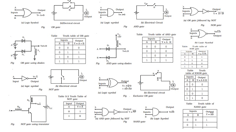
(i) OR gate
An OR gate has two or more inputs
but only one output. It is known as OR gate, because the output is high if any
one or all of the inputs are high. The logic symbol of a two input OR gate is
shown in Fig a.
The Boolean
expression to represent OR gate is given by Y= A+B (+ symbol should be read as
OR)
The OR gate can be thought of like an electrical circuit shown
in Fig b, in which switches are connected in parallel with each other. The lamp
will glow if both the inputs are closed or any one of them is closed.
Diode OR gate
Fig shows a simple circuit using diodes to build a two input OR
gate. The working of this circuit can be explained as follows.
Case (i) A = 0 and B = 0
When both A and B are at zero level, (i.e.) low, the output
voltage will be low, because the diodes are non-conducting.
Case (ii) A = 0 and B = 1
When A is low and B is high, diode D2 is forward
biased so that current flows through RL and output is high.
Case (iii) A = 1 and B = 0
When A is high and B is low, diode D1 conducts and the
output is high.
Case (iv) A = 1 and B = 1
When A and B both are high, both
diodes D1 and D2 are conducting and the output is high.
Therefore Y is high. The OR gate operations are shown in Table
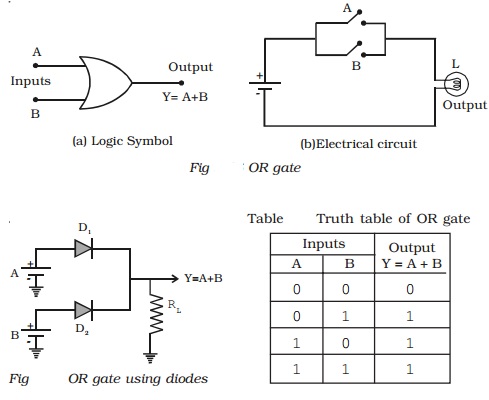
(ii) AND gate
An AND gate has two or more inputs but only one output. It is
known as AND gate because the output is high only when all the inputs are high.
The logic symbol of a two input AND gate is shown in Fig a.
Y = A⋅B ( ⋅ should be read as AND)
AND gate may be thought of an
electrical circuit as shown in Fig b, in which the switches are connected in
series. Only if A and B are closed, the lamp will glow, and the output is high.
Diode AND gate
Fig shows a simple
circuit using diodes to build a two-input AND gate. The working of the circuit
can be explained as follows :
Case (i) A = 0 and B = 0
When A and B are zero, both
diodes are in forward bias condition and they conduct and hence the output will
be zero, because the supply voltage VCC will be dropped across RL
only. Therefore Y = 0.
Case (ii) A = 0 and B = 1
When A = 0 and B is high, diode D1
is forward biased and diode D2 is reverse biased. The diode D1
will now conduct due to forward biasing. Therefore, output Y = 0.
Case (iii) A = 1 and B = 0
In this case, diode D2
will be conducting and hence the output Y = 0.
Case (iv) A = 1 and B = 1
In this case, both the diodes are
not conducting. Since D1 and D2 are in OFF condition, no
current flows through RL. The output is equal to the supply voltage.
Therefore Y = 1.
Thus the output will be high only
when the inputs A and B are high. The Table 9.2 summarises the function of an
AND gate.
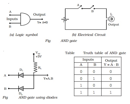
(iii) NOT gate (Inverter)
The NOT gate is a gate with only one input and one output. It is
so called, because its output is complement to the input. It is also known as
inverter. Fig a shows the logic symbol for NOT gate.
The Boolean expression to
represent NOT operation is Y = A .
The NOT gate can be thought of
like an electrical circuit as shown in Fig b. When switch A is closed, input is
high and the bulb will not glow (i.e) the output is low and vice versa.
Fig is a transistor in CE
mode, which is used as NOT gate. When the input A is high, the transistor is
driven into saturation and hence the output Y is low. If A is low, the
transistor is in cutoff and hence the output Y is high. Hence, it is seen that
whenever input is high, the output is low and vice versa. The operation of NOT
gate is shown in Table 9.3.
Exclusive OR gate (EXOR gate)
The logic symbol for exclusive OR (EXOR) gate is shown in
The Boolean expression to represent EXOR operation is
Y = A ⊕ B
EXOR gate has an output 1, only when the inputs are complement
to each other.
The equivalent switching circuit is shown in Fig b.
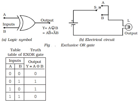
Switch positions A and B will individually make the lamp to be
ON. But the combination of A and B is not possible.
The EXOR operation is represented in Table.
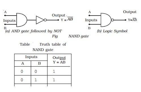
NAND gate
This is a NOT-AND gate. It can be obtained by connecting a NOT
gate at the output of an AND gate (Fig a).
The logic symbol for NAND gate is shown in Fig b.
NAND gate function is reverse of AND gate function. A NAND gate
will have an output,
only if both inputs are not 1. In other words, it gives an
output 1, if either A or B or both are 0. The
operation of a NAND gate is represented in Table.
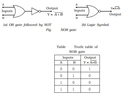
NOR gate
This is a NOT-OR gate. It can be made out of an OR gate by
connecting an inverter at its output (Fig a).
The logic symbol for NOR gate is given in Fig b
The NOR gate function is the reverse of OR gate function. A NOR
gate will have an output, only when all inputs are 0. In a NOR gate, output is
high, only when all inputs are low. The NOR operation is represented in Table.
Related Topics