Chapter: Digital Logic Circuits : Synchronous Sequential Circuits
Analysis and Design of Sequential Circuits
Analysis of Sequential Circuits
The behaviour of a sequential circuit is
determined from the inputs, the outputs and the states of its flip-flops. Both
the output and the next state are a function of the inputs and the present
state.
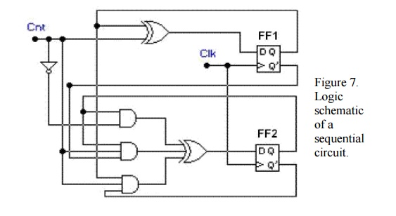
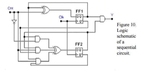
Derive the state table and state diagram for the
sequential circuit shown in Figure 7.
SOLUTION:
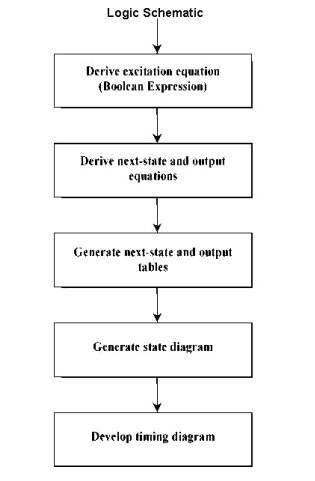
STEP 1: First we derive the Boolean expressions
for the inputs of each flip-flops in the schematic, in terms of external input
Cnt and the flip-flop outputs Q1 and Q0. Since there are two D flip-flops in
this example, we derive two expressions for D1 and D0:
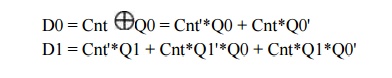
These Boolean expressions are called excitation
equations since they represent the inputs to the flip-flops of the sequential
circuit in the next clock cycle.
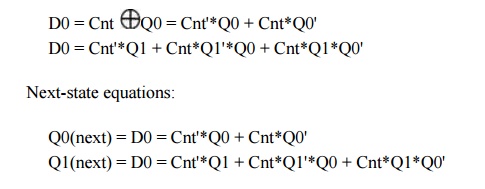
STEP 2: Derive the next-state equations by
converting these excitation equations into flip-flop characteristic equations.
In the case of D flip-flops, Q(next) = D. Therefore the next state
equal the excitation equations.
Q0(next) = D0 = Cnt'*Q0
+ Cnt*Q0'
Q1(next) = D1 = Cnt'*Q1
+ Cnt*Q1'*Q0 + Cnt*Q1*Q0'
STEP 3: Now convert these next-state equations
into tabular form called the next-state table.
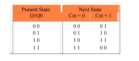
Each row is corresponding to a state of the
sequential circuit and each column represents one set of input values. Since we
have two flip-flops, the number of possible states is four - that is, Q1Q0
can be equal to 00, 01, 10, or 11. These are present states as shown in the
table.
For the next state part of the table, each entry
defines the value of the sequential circuit in the next clock cycle after the
rising edge of the Clk. Since this value depends on the present state and the
value of the input signals, the next state table will contain one column for
each assignment of binary values to the input signals. In this example, since
there is only one input signal, Cnt, the next-state table shown has only two
columns, corresponding to Cnt = 0 and Cnt = 1.
Note that each entry in the next-state table
indicates the values of the flip-flops in the next state if their value in the
present state is in the row header and the input values in the column header.
Each of these next-state values has been computed
from the next-state equations in STEP 2.
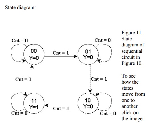
STEP 4: The state diagram is generated directly
from the next-state table, shown in Figure 8.
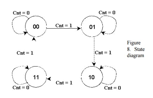
Each arc is labelled with the values of the
input signals that cause the transition from the present state (the source of
the arc) to the next state (the destination of the arc).
In general, the number of states in a next-state
table or a state diagram will equal 2m , where m is the number of flip-flops.
Similarly, the number of arcs will equal 2m x 2k , where k is the number of
binary input signals. Therefore, in the state diagram, there must be four
states and eight transitions. Following these transition arcs, we can see that
as long as Cnt = 1, the sequential circuit goes through the states in the
following sequence: 0, 1, 2, 3, 0, 1, 2, .... On the other hand, when Cnt = 0,
the circuit stays in its present state until Cnt changes to 1, at which the
counting continues.
Since this sequence is characteristic of
modulo-4 counting, we can conclude that the sequential circuit in Figure 7 is a
modulo-4 counter with one control signal, Cnt, which enables counting when Cnt
= 1 and disables it when Cnt = 0.
To see how the states changes corresponding to
the input signals Cnt, click on this image.
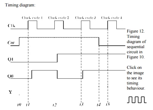
Below, we show a timing diagram, representing
four clock cycles, which enables us to observe the behaviour of the counter in
greater detail.
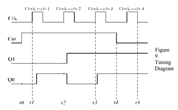
In this timing diagram we have assumed that Cnt
is asserted in clock cycle 0 at t0 and is disasserted in clock cycle 3 at time
t4. We have also assumed that the counter is in state Q1Q0 = 00 in the clock
cycle 0. Note that on the clock's rising edge, at t1, the counter will go to
state Q1Q0 = 01 with a slight propagation delay; in cycle 2, after t2, to Q1Q0
= 10; and in cycle 3, after t3 to Q1Q0 = 11. Since Cnt becomes 0 at t4, we know
that the counter will stay in state Q1Q0 = 11 in the next clock cycle. To see
the timing behaviour of the circuit click on this image

In Example 1.1 we demonstrated the analysis of a
sequential circuit that has no outputs by developing a next-state table and
state diagram which describes only the states and the transitions from one
state to the next. In the next example we complicate our analysis by adding
output signals, which means that we have to upgrade the next-state table and
the state diagram to identify the value of output signals in each state.
SOLUTION:
The input combinational logic in Figure 10 is
the same as in Example 1.1, so the excitation and the next-state equations will
be the same as in Example 1.1.
Excitation equations:
In addition, however, we have computed the
output equation.
Output equation: Y = Q1Q0
As this equation shows, the output Y will equal
to 1 when the counter is in state Q1Q0 = 11, and it will stay 1 as long as the
counter stays in that state.
Next-state and output table:
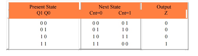
Note that the counter will reach the state Q1Q0
= 11 only in the third clock cycle, so the output Y will equal 1 after Q0
changes to 1. Since counting is disabled in the third clock cycle, the counter
will stay in the state Q1Q0 = 11 and Y will stay asserted in all succeeding
clock cycles until counting is enabled again.
Design of Sequential Circuits
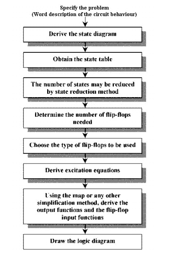
The design of a synchronous sequential circuit
starts from a set of specifications and culminates in a logic diagram or a list
of Boolean functions from which a logic diagram can be obtained. In contrast to
a combinational logic, which is fully specified by a truth table, a sequential
circuit requires a state table for its specification. The first step in the
design of sequential circuits is to obtain a state table or an equivalence
representation, such as a state diagram.
A synchronous sequential circuit is made up of flip-flops
and combinational gates. The design of the circuit consists of choosing the
flip-flops and then finding the combinational structure which, together with
the flip-flops, produces a circuit that fulfils the required specifications.
The number of flip-flops is determined from the number of states needed in the
circuit.
The recommended steps for the design of
sequential circuits are set out below.
Related Topics