Chapter: Microprocessor and Microcontroller : 8086 System Bus Structure
80286 Microprocessor
Advanced
processors: 80286 Microprocessor
Salient Features of 80286
ü The 80286
is the first member of the family of advanced microprocessors with memory
management and protection abilities. The 80286 CPU, with its 24-bit address bus
is able to address 16 Mbytes of physical memory. Various versions of 80286 are
available that runs on 12.5 MHz, 10 MHz and 8 MHz clock frequencies. 80286 is
upwardly compatible with 8086 in terms of instruction set.
ü 80286 has
two operating modes namely real address mode and virtual address mode. In real
address mode, the 80286 can address upto 1Mb of physical memory address like
8086. In virtual address mode, it can address up to 16 Mb of physical memory
address space and 1 GB of virtual memory address space.
ü The
instruction set of 80286 includes the instructions of 8086 and 80186. 80286 has
some extra instructions to support operating system and memory management. In
real address mode, the 80286 is object code compatible with 8086. In protected
virtual address mode, it is source code compatible with 8086. The performance
of 80286 is five times faster than the standard 8086.
Need for Memory Management
The part
of main memory in which the operating system and other system programs are
stored is not accessible to the users. It is required to ensure the smooth
execution of the running process and also to ensure their protection. The
memory management which is an important task of the operating system is
supported by a hardware unit called memory management unit.
Swapping in of the Program
Fetching
of the application program from the secondary memory and placing it in the
physical memory for execution by the CPU.
Swapping out of the executable
Program
Saving a
portion of the program or important results required for further execution back
to the secondary memory to make the program memory free for further execution
of another required portion of the program.
Concept of Virtual Memory
Large
application programs requiring memory much more than the physically available
16 Mbytes of memory, may be executed by diving it into smaller segments. Thus
for the user, there exists a very large logical memory space which is not
actually available. Thus there exists a virtual memory which does not exist
physically in a system. This complete process of virtual memory management is
taken care of by the 80286 CPU and the supporting operating system.
Internal Architecture of 80286
Register Organization of 80286
The 80286
CPU contains almost the same set of registers, as in 8086, namely
1. Eight
16-bit general purpose registers
2. Four
16-bit segment registers
3. 3. Status
and control registers
4. 4.Instruction
Pointer
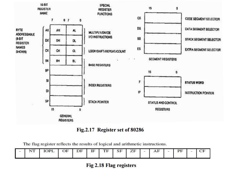
D2, D4,
D6, D7 and D11 are called as status flag bits. The bits D8 (TF) and D9 (IF) are
used for controlling machine operation and thus they are called control flags.
The additional fields available in 80286 flag registers are:
1. IOPL -
I/O Privilege Field (bits D12 and D13)
2. NT -
Nested Task flag (bit D14)
3. PE -
Protection Enable (bit D16)
4. MP -
Monitor Processor Extension (bit D17)
5. EM -
Processor Extension Emulator (bit D18)
6. TS – Task
Switch (bit D19)
Protection
Enable flag places the 80286 in protected mode, if set. This can only be
cleared by resetting the CPU. If the Monitor Processor Extension flag is set,
allows WAIT instruction to generate a processor extension not present
exception.
Processor
Extension Emulator flag if set, causes a processor extension absent exception
and permits
the
emulation of processor extension by the CPU.
Task
Switch flag if set, indicates the next instruction using extension will
generate exception 7, permitting the CPU to test whether the current processor
extension is for the current task.
Machine Status Word (MSW)
The
machine status word consists of four flags – PE, MO, EM and TS of the four
lower order bits D19 to D16 of the upper word of the flag register. The LMSW
and SMSW instructions are available in the instruction set of 80286 to write
and read the MSW in real address mode.
Internal Block Diagram of 80286
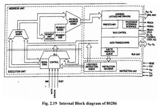
The CPU
contain four functional blocks
1. Address
Unit (AU)
2. Bus Init
(BU)
3. Instruction
Unit (IU)
4. Execution
Unit (EU)
The
address unit is responsible for calculating the physical address of
instructions and data that the CPU wants to access. Also the address lines
derived by this unit may be used to address different peripherals. The physical
address computed by the address unit is handed over to the bus unit (BU) of the
CPU. Major function of the bus unit is to fetch instruction bytes from the
memory. Instructions are fetched in advance and stored in a queue to enable
faster execution of the instructions. The bus unit also contains a bus control
module that controls the prefetcher module. These prefetched instructions are
arranged in a 6-byte instructions queue. The 6-byte prefetch queue forwards the
instructions arranged in it to the instruction
unit (IU). The instruction unit accepts instructions from the prefetch
queue and an instruction decoder
decodes
them one
by one. The decoded instructions are latched onto a decoded instruction queue.
The output of the decoding circuit drives a control circuit in the execution unit, which is responsible
for executing the instructions received from decoded instruction queue. The
decoded instruction queue sends the data part of the instruction over the data
bus. The EU contains the register bank used for storing the data as scratch
pad, or used as special purpose registers. The ALU, the heart of the EU,
carries out all the arithmetic and logical operations and sends the results
over the data bus or back to the register bank.
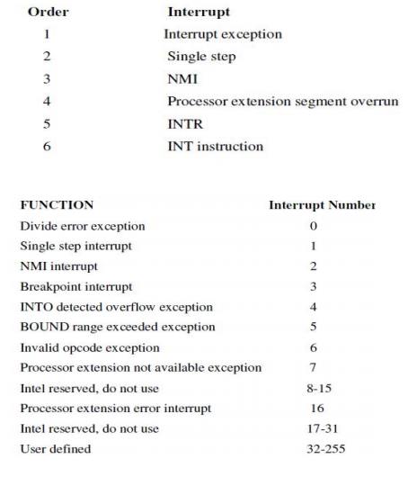
Interrupts of 80286
The
Interrupts of 80286 may be divided into three categories,
1. External
or hardware interrupts
2. INT
instruction or software interrupts
3. Interrupts
generated internally by exceptions
While
executing an instruction, the CPU may sometimes be confronted with a special
situation because of which further execution is not permitted. While trying to
execute a divide by zero instruction, the CPU detects a major error and stops further
execution. In this case, we say that an exception has been generated. In other
words, an instruction exception is an unusual situation encountered during
execution of an instruction that stops further execution. The return address
from an exception, in most of the cases, points to the instruction that caused
the exception.
As in the
case of 8086, the interrupt vector table of 80286 requires 1Kbytes of space for
storing 256, four-byte pointers to point to the corresponding 256 interrupt
service routines (lSR). Each pointer contains a 16-bit offset followed by a
16-bit segment selector to point to a particular ISR. The calculation of vector
pointer address in the interrupt vector table from the (8-bit) INT type is
exactly similar to 8086.
Like
8086, the 80286 supports the software interrupts of type 0 (INT 00) to type FFH
(INT FFH).
Maskable Interrupt INTR: This is a
maskable interrupt input pin of which the INT type is to be provided by an external circuit like an interrupt
controller. The other functional details of this interrupt pin are exactly
similar to the INTR input of 8086.
Non-Maskable Interrupt NMI: It has
higher priority than the INTR interrupt.
Whenever
this interrupt is received, a vector value of 02 is supplied internally to
calculate the pointer to the interrupt vector table. Once the CPU responds to a
NMI request, it does not serve any other interrupt request (including NMI).
Further it does not serve the processor extension (coprocessor) segment overrun
interrupt, till either it executes IRET or it is reset. To start with, this
clears the IF flag which is set again with the execution of IRET, i.e. return
from interrupt.
Single Step Interrupt
As in
8086, this is an internal interrupt that comes into action, if trap flag (TF) of 80286 is set. The CPU
stops the execution after each instruction cycle so that the register contents
(including flag register), the program status word and memory, etc. may be
examined at the end of each instruction execution. This interrupt is useful for
troubleshooting the software. An interrupt vector type 01 is reserved for this
interrupt.
Interrupt Priorities:
If more
than one interrupt signals occur simultaneously, they are processed according
to their priorities as shown below:
Signal Description of 80286
CLK: This is the system clock input
pin. The clock frequency applied at this pin is divided by two internally and is used for deriving fundamental timings for
basic operations of the circuit. The clock is generated using 8284 clock
generator.
D15-D0: These are sixteen bidirectional
data bus lines.
A23-A0: These are the physical address
output lines used to address memory or I/O devices. The address lines A23 - A16 are zero during I/O transfers
BHE: This output signal, as in 8086,
indicates that there is a transfer on the higher byte of the data bus (D15 – D8) .
S1 , S0: These are the active-low status output signals which indicate
initiation of a bus cycle and with
M/IO and COD/INTA, they define the type of the bus cycle.
M/ IO: This output line differentiates
memory operations from I/O operations. If this signal is it “0” indicates that an I/O cycle or INTA cycle is in process
and if it is “1” it indicates
that a
memory or a HALT cycle is in progress.
COD/ INTA: This output signal, in
combination with M/ IO signal and S1 , S0
distinguishes different memory, I/O and INTA cycles.
LOCK: This active-low output pin is
used to prevent the other masters from gaining the control of the bus for the current and the following bus cycles.
This pin is activated by a "LOCK" instruction prefix, or
automatically by hardware during XCHG, interrupt acknowledge or descriptor
table access
READY This active-low input pin is used
to insert wait states in a bus cycle, for interfacing low speed peripherals. This signal is neglected during HLDA cycle.
HOLD and HLDA This pair of pins is used by
external bus masters to request for the control
of the system bus (HOLD) and to check whether the main processor has granted
the control (HLDA) or not, in the same way as it was in 8086.
INTR: Through this active high input,
an external device requests 80286 to suspend the current instruction execution and serve the interrupt request. Its
function is exactly similar to that of INTR pin of 8086.
NMI: The Non-Maskable Interrupt
request is an active-high, edge-triggered input that is equivalent to an INTR signal of type 2. No acknowledge cycles are
needed to be carried out.
PEREG and PEACK (Processor Extension
Request and Acknowledgement)
Processor
extension refers to coprocessor (80287 in case of 80286 CPU). This pair of pins
extends the memory management and protection capabilities of 80286 to the
processor extension 80287. The PEREQ input requests the 80286 to perform a data
operand transfer for a processor extension. The PEACK active-low output
indicates to the processor extension that the requested operand is being
transferred.
BUSY and ERROR: Processor extension BUSY and
ERROR active-low input signals indicate
the operating conditions of a processor extension to 80286. The BUSY goes low,
indicating 80286 to suspend the execution and wait until the BUSY become
inactive. In this duration, the processor extension is busy with its allotted
job. Once the job is completed the processor extension drives the BUSY input
high indicating 80286 to continue with the program execution. An active ERROR
signal causes the 80286 to perform the processor extension interrupt while
executing the WAIT and ESC instructions. The active ERROR signal indicates to
80286 that the processor extension has committed a mistake and hence it
is
reactivating the processor extension interrupt.
CAP: A 0.047
μf, 12V capacitor must be connected between this input pin and ground to filter the output of the internal
substrate bias generator. For correct operation of 80286 the capacitor must be
charged to its operating voltage. Till this capacitor charges to its full
capacity, the 80286 may be kept stuck to reset to avoid any spurious activity.
Vss: This pin
is a system ground pin of 80286.
Vcc: This pin
is used to apply +5V power supply voltage to the internal circuit of 80286. RESET The active-high RESET input
clears the internal logic of 80286, and reinitializes it RESET The active-high reset input pulse width should be at least 16
clock cycles. The 80286 requires at
least 38 clock cycles after the trailing edge of the RESET input signal, before
it makes the first opcode fetch cycle.
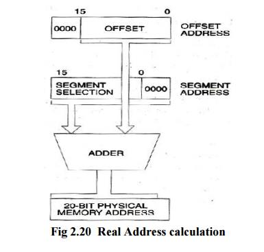
Real Address Mode
• Act as a
fast 8086
• Instruction
set is upwardly compatible
• It
address only 1 M byte of physical memory using A0-A19.
• In real
addressing mode of operation of 80286, it just acts as a fast 8086. The
instruction
set is upward compatible with that of 8086.
The 80286
addresses only 1Mbytes of physical memory using A0- A19. The lines A20-A23 are
not used by the internal circuit of 80286 in this mode. In real address mode,
while addressing the physical memory, the 80286 uses BHE along with A0- A19.
The 20-bit physical address is again formed in the same way as that in 8086.
The contents of segment registers are used as
segment base addresses. The other registers, depending upon the addressing
mode, contain the offset addresses. Because of extra pipelining and other
circuit level improvements, in real address mode also, the 80286 operates at a
much faster rate than 8086, although functionally they work in an identical
fashion. As in 8086, the physical memory is organized in terms of segments of
64Kbyte maximum size.
An exception is generated, if the segment size
limit is exceeded by the instruction or the data. The overlapping of physical
memory segments is allowed to minimize the memory requirements for a task. The
80286 reserves two fixed areas of physical memory for system initialization and
interrupt vector table. In the real mode the first 1Kbyte of memory starting
from address 0000H to 003FFH is reserved for interrupt vector table. Also the
addresses from FFFF0H to FFFFFH are reserved for system initialization.
The
program execution starts from FFFFH after reset and initialization. The
interrupt vector table of 80286 is organized in the same way as that of 8086.
Some of the interrupt types are reserved for exceptions, single-stepping and
processor extension segment overrun, etc.
When the
80286 is reset, it always starts the execution in real address mode. In real
address mode, it performs the following functions: it initializes the IP and
other registers of 80286, it prepares for entering the protected virtual
address mode.
Protected Virtual Address Mode (PVAM)
80286 is
the first processor to support the concepts of virtual memory and memory
management. The virtual memory does not exist physically it still appears to be
available within the system. The concept of VM is implemented using Physical
memory that the CPU can directly access and secondary memory that is used as a
storage for data and program, which are stored in secondary memory initially.
The
Segment of the program or data required for actual execution at that instant is
fetched from the secondary memory into physical memory. After the execution of
this fetched segment, the next segment required for further execution is again
fetched from the secondary memory, while the results of the executed segment
are stored back into the secondary memory for further references. This continues
till the complete program is executed
During
the execution the partial results of the previously executed portions are again
fetched into the physical memory, if required for further execution. The
procedure of fetching the chosen program segments or data from the secondary
storage into physical memory is called swapping.
The procedure of storing back the partial results or data back on the secondary
storage is called unswapping. The
virtual memory is allotted per task.
The 80286
is able to address 1 G byte (230 bytes) of virtual memory per task. The
complete virtual memory is mapped on to the 16Mbyte physical memory. If a
program larger than 16Mbyte is stored on the hard disk and is to be executed,
if it is fetched in terms of data or program segments of less than 16Mbyte in
size into the program memory by swapping sequentially as per sequence of
execution.
Whenever
the portion of a program is required for execution by the CPU, it is fetched
from the secondary memory and placed in the physical memory is called swapping in of the program. A portion of the program or important partial
results required for further execution,
may be saved back on secondary storage to make the PM free for further
execution of another required portion of the program is called swapping out of the executable program.
80286
uses the 16-bit content of a segment register as a selector to address a
descriptor stored in the physical memory. The descriptor is a block of
contiguous memory locations containing information of a segment, like segment
base address, segment limit, segment type, privilege level, segment
availability in physical memory, descriptor type and segment use another task.
Related Topics